Ceva is a very focused company. In its words, the leader in innovative silicon and software IP solutions that enable smart edge products to connect, sense, and infer data more reliably and efficiently. You can see some of its accomplishments here. The company has been licensing IP for more than twenty years with more than 17 billion Ceva-powered devices shipped, including more than 1.6 billion devices in 2023. Impressive. Thanks to the growing popularity of intelligent products and the massive data created by ubiquitous sensor networks to drive those products, edge computing has become a key element to deliver new innovation. Recently, Ceva made an announcement at Embedded World in Nuremberg, Germany. The announcement has significant implications for IoT and Smart Edge AI Applications. In this post, I’ll summarize the announcement and take a closer look at the underlying technology to see how Ceva accelerates IoT and smart edge AI with a new wireless platform IP family.
The Announcement
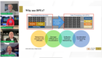
At the center of the announcement was the Ceva-Waves™ Links™ IP Family. This new product family delivers fully integrated multi-protocol connectivity solutions with Wi-Fi, Bluetooth, UWB, Thread, Zigbee, and Matter. By covering all those protocols in one architecture, development is simplified and time to market is accelerated for next generation, connectivity rich, MCUs and SoCs. Momentum for the product line begins with the introduction of Ceva-Waves Links100, an IoT-focused connectivity platform IP with RF implemented on TSMC 22nm. This platform is currently being deployed by a leading OEM customer.
The new IP family finds application in the consumer IoT, industrial, automotive, and personal computing markets. A key feature of the family is the wide protocol support – Wi-Fi, Bluetooth, Ultra-Wideband (UWB), and IEEE 802.15.4 (for Thread / Zigbee / Matter). This delivers a range of qualified, easy-to-integrate, multi-protocol wireless communications subsystems, featuring optimized co-existence schemes and adapted to various radios and configurations. The demand for smaller, low-cost, high-performance devices is driving the need to consolidate multiple connectivity protocols in a single chip. ABI Research has discussed the move from module-level integration to on-die chip integration and forecasts that Wi-Fi plus Bluetooth combo chipset shipments will approach 1.6 billion chips annually by 2028.
In the release, Tal Shalev, Vice President and General Manager of the Wireless IoT BU at CEVA commented:
“The Ceva-Waves Links wireless connectivity IPs build on our extensive portfolio that already powers more than 1 billion devices annually and has enabled us to establish a strong and diversified customer base across consumer and industrial IoT applications. With many customers designing chips employing multiple wireless standards, Links is a natural extension, leveraging our technology and expertise to dramatically reduce the technology barrier but yet delivering a tailored, optimal solution that provides the high-performance, low latency and low-power connectivity required.”
The first member of the Ceva-Waves Links family is the Links100, an integrated, low power, Wi-Fi / Bluetooth / 802.15.4 communications subsystem IP for IoT applications. You can read the complete press release here.
A Closer Look at the Ceva-Waves Links IP Family
First, a bit of history regarding product family designations. The Ceva Connectivity IP Family is now unified under Ceva-Waves™ solutions. This includes products such as Ceva-Waves™ Bluetooth (supporting also IEEE 802.15.4), Ceva-Waves WiFi, and Ceva-Waves UWB. The announcement introduces Ceva’s multi-protocol wireless combo platform family, Ceva-Waves Links.
Regarding protocols, each standard has its own strengths. A quick profile is useful:
- Bluetooth is the most widespread low power wireless connectivity used to transfer small amounts of data for a broad range of applications such as mobile, wearable, hearable, smart home, connected home, medical, automotive, and IoT.
- Wi-Fi is the most widespread wireless technology to connect devices to the internet used to transfer small to big amounts of data for a broad range of applications such as mobile, wearable, smart home, connected home, medical, automotive, and IoT.
- IEEE 802.15.4 is a popular low power wireless technology to connect devices to transfer small amounts of data in applications such as smart home and IoT. It is the underlying technology used for Thread, Matter and Zigbee.
- UWB introduces a new realm of spatial awareness with the most accurate and secure ranging, Android Open Accessory (AoA) support, and radar sensing capabilities. It is used in a wide range of applications such as automotive, wearables, asset tracking, find-me, indoor navigation, and payments.
Combining multiple protocols in one IP family has significant benefits. These include:
- Lower-cost – incorporating multiple wireless standards in a chip reduces the bill of material with less components, lower size, and smaller PCB
- Lower-power – incorporating multiple wireless standards and RF in a single chip reduces the power consumption thanks to resource sharing and co-existence optimization
- Fast, simple and risk free – replacing a few components by a single integrated chip accelerates time to market, simplifies the design, and reduces the risks of mistake and bad performance
- Higher co-existence performance – instead of having separate wireless chips, embedding all in a single component enables richer co-existence interfaces leading to higher performance multi-protocol scenarios
- Versatility for future-proofing – supporting multiple wireless standards ensures longevity and compatibility with evolving connectivity requirements for a wide range of use cases
Digging a bit deeper, Ceva-Waves Links delivers a family of integrated, multi-protocol wireless communication platforms. As discussed, the family is built on the core connectivity technologies of Bluetooth, 802.15.4, Wi-Fi, and UWB. This provides a seamless end-to-end solution, from radio to upper software stacks.
The product family features optimized co-existence schemes for seamless protocol integration and is adaptable to a range of radios, either from partners or provided by Ceva. The family is designed with a modular architecture, enabling unique customization, targeting a variety of use cases and markets for unparalleled versatility. The diagram to the right summarizes the family architecture.
Ceva-Waves Links100 is the first available member of the new family. It is a fully integrated wireless platform IP designed for low-power applications, combining hardware and software for Wi-Fi 6 1×1, Bluetooth 5.4 dual-mode, and 802.15.4 (for ZigBee, Thread and Matter). It contains a 2.4GHz RF transceiver in 22nm technology, shared between Bluetooth, 802.15.4 and Wi-Fi operations.
This delivers a smart co-existence scheme for multi-protocol traffic, with a complete software suite for easy deployment. As mentioned, the product is currently being deployed by a leading OEM customer. The diagram to the right summarizes the Links100 architecture.
To Learn More
You can learn more about the Ceva-Waves Links IP Platforms here. More information is also available regarding Ceva’s support for Wi-Fi, Bluetooth, and Ultra-Wideband (UWB). And that’s how Ceva accelerates IoT and smart edge AI with a new wireless platform IP family.