
Embracing cloud computing is highly attractive for users of electronic design automation (EDA) tools and flows because of the productivity gains and time to market advantages that it can offer. For Siemens EDA customers engaged in designing large, cutting-edge chips at advanced nanometer scales, running Calibre® design stage and signoff verification in the cloud proves advantageous, as evidenced by the benchmark results discussed in this article. Calibre flows not only facilitate swift design iterations with modest compute resources but also consistently improve with each release. Cloud deployment offers a dual benefit: design teams avoid waiting for local resources and gain the flexibility to scale up during peak demand and leverage Calibre’s scalability for increased design throughput.
But to be cost-effective, cloud resources and infrastructure must be tailored to meet the individual and diverse demands of the many tools that constitute the semiconductor design flow. So what is the optimal configuration for running Calibre applications in the cloud? Which of the dozens of classes of virtual machines are best for running Calibre applications? How do cloud users know they are spending their money wisely and getting the best results? We set out to answer all these questions with a collaboration between Amazon Web Services (AWS), Amazon Annapurna Labs (Annapurna) and Siemens EDA to evaluate results from a series of Calibre flow benchmarks run inside Annapurna’s production virtual private cloud (VPC), which is hosted on AWS. After this evaluation, we developed a set of best known methods (BKMs) based on our experiences and the results.
Environment setup
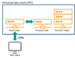
The cloud experience works best when it is configured to be seamless from an end-user’s perspective. The setup that is probably most familiar to semiconductor designers in their on-premises systems is one where user has an exclusive small head node assigned that is used to submit all their jobs to other machines using some kind of queue manager. The head node is also useful for housekeeping purposes, like editing files, moving data, capturing metrics, etc.
The Calibre nmDRC benchmarks detailed in this paper took advantage of the Calibre MTFlex distributed processing mode running on a primary machine with a series of attached remote machines. In these cases, we used the same machine type for both the remote hosts and the primary. Other tests simply used multithreading on a single machine. A virtual private cloud setup is illustrated in figure 1.
Calibre nmDRC benchmark results
Figure 2 shows results for Calibre nmDRC runtime and peak remote memory usage for an Annapurna 7nm design when using an increasing number of remote cores. Runtime is shown in hours, and peak remote memory usage in GB. All runs used the Calibre MTflex distributed processing mode and a homogeneous cluster of machine types for the primary and remote nodes (AWS r6i.32xlarge instances). The horizontal axis shows the number of remote cores, which were doubled with each subsequent run. Each run used a consistent 64-core primary machine.
The dark blue line is the baseline run using the same Calibre nmDRC version that Annapurna originally used in production on these designs with stock rules from their foundry partner. The light green line shows results using a more recent Calibre nmDRC version with optimized rules and instead of reading the data in from an OASIS file, the design data was restored from a previously saved reusable hierarchical database (RHDB) which in this case saved about 20 minutes per run. The light blue dotted line shows the percentage time saving between these two sets of runs. The purple line is the Calibre nmDRC Recon run, which automatically selects a subset of the foundry rules to run to find and resolve early design iteration systematic errors. Siemens EDA always recommends that customers run the Calibre nmDRC Recon tool on dirty designs before committing to a full Calibre run. This helps find the gross errors in the design very quickly, so they can be eliminated with short cycle times.
Determining how many remote cores to use in the cloud is dependent on the size and complexity of the design, the process technology, and the complexity of the rule deck. The optimal spot is found around the “knee” in the curve on these charts (for the design in figure 2, around 500 remote cores). The peak memory plots show that there was plenty of headroom for physical memory – each remote had 1TB RAM. The cost of these runs is typically in the range of a couple hundred dollars. Calibre customers typically use 500 remote cores as a minimum for full-chip Calibre nmDRC runs at advanced nodes. The data supports the Calibre value proposition of maintaining fast turnaround based on a modest amount of compute resource. However, the data also shows that scalability continues to even greater numbers of cores, giving Calibre users headroom to further compress cycle time if needed.
Figure 3 shows similar results for a Calibre nmDRC run on a 5nm Annapurna design. Here again, the optimal spot is around 500 remote cores, with fewer than 5 hours of runtime.
Here again, the data demonstrates that the Calibre nmDRC tool is very resource-efficient, so it is not necessary to use thousands of remote CPUs to get reasonable design cycle times. Design teams can readily perform multiple turns per day using a modest number of cores, with a correspondingly modest associated cost. If it is helpful or necessary to squeeze in one or two more design turns per day, they can increase the number to 1,000 remote cores. The advantage of operating in the cloud is that more machines are always available, and it is highly likely that they will spin up very quickly.
Calibre interactive run management results
Both Annapurna designs were opened in the Calibre DESIGNrev interface, and the Calibre Interactive invocation GUI was used to initiate Calibre nmDRC and Calibre nmLVS runs. In addition, the Calibre Interactive integration with the Altair Accelerator (NC) queue manager was assessed, and Calibre RVE invocation and cross-probing to the design in the Calibre DESIGNrev interface was evaluated. All Calibre Interactive operations were fast and responsive.
Best known methods for EDA cloud computing
Following the benchmarks, we evaluated the results to encapsulate learnings and observations into suggested BKMs for running Calibre applications in the cloud. We generated general BKMs for optimizing spend in the cloud, improving cloud performance, and optimizing the general experience when using cloud-based resources, as well a specific BKMs for running Calibre flows in the cloud. These BKMs are encapsulated as Cloud Flight Plans, which are instructions for flow-specific optimizations that will allow Siemens EDA customers to leverage the availability, scalability and flexibility of cloud compute in a way that is very cost effective. Many of these resources are available through cloud landing pages on our Siemens EDA website. Our Cloud Reference Environment and other flow-specific assets and resources are available to our customers through our SupportCenter resource site.
Download our newest technical paper that describes BKMs for Amazon Web Services (AWS), using Annapurna Labs’ experience as a benchmark. Running Calibre solutions in the cloud: Best known methods.
Conclusion
In the realm of electronic design automation (EDA), cloud computing offers a compelling solution to the problem of constantly burgeoning design size and complexity. Design teams, armed with cloud-tuned machines, can work at an accelerated pace—launching jobs when needed, utilizing resources efficiently, and even running multiple tasks in parallel. Whether it’s accelerating design cycles or optimizing costs, the cloud provides flexibility. To navigate this celestial landscape effectively, understanding and optimizing cloud resources and configurations is key. Siemens EDA, in collaboration with major cloud providers like AWS, has crafted Cloud Flight Plans to guide design mutual customers on their cloud journey. With Cloud Flight Plans as their compass, semiconductor designers can chart a steady course toward efficient, cloud-powered success.
Also Read:
Solido Siemens and the University of Saskatchewan
Three New Circuit Simulators from Siemens EDA
Siemens Provides a Complete 3D IC Solution with Innovator3D IC


