We at Semiconductor Intelligence estimate the automotive semiconductor market was $67 billion in 2023, up 12% from 2022. The top twelve suppliers accounted for over three-quarters of the market. Infineon Technologies was the largest automotive semiconductor supplier, at $9.2 billion or 13.7% of the market. NXP Semiconductors was second at 11.2% and STMicroelectronics was third at 10.6%. These top three companies accounted for over one-third of the market. For most of these companies, automotive is a significant part of their total revenues. Of the top six companies, the percentage of revenues from automotive ranged from 34% to 56%.
The automotive semiconductor industry has shown strong growth since 2021 as the industry bounced back from pandemic-related shortages. However, there are signs of a slowdown in the market. The quarterly automotive semiconductor revenue of the top three suppliers reflects this trend. Infineon reported strong growth through 2022 and early 2023 but peaked in 2Q 2023 and has been declining since. Though Infineon’s automotive revenue guidance for 2Q 2024 is for 5% quarter-to-quarter growth. NXP saw quarter-to-quarter revenue growth through 4Q 2023 but reported a 5% decline in 1Q 2024. NXP’s 1Q 2024 report cited continued inventory reductions and a soft overall automotive market in the first half of 2024. ST’s quarter-to-quarter revenue growth was strong in 2022 and 2023, averaging 7%. That growth ended in 1Q 2024 when ST reported a 23% decline in automotive revenue, citing a “deceleration phase”.
Motor vehicle production in 2023 was 93.5 million units, according to the International Organization of Motor Vehicle Manufacturers (OICA), up 10% from 2022. This was the strongest production growth since 26% in 2010 during the recovery from the great recession of 2008-2009. The 93.5 million vehicles in 2023 were still below the all-time high of 97.3 million vehicles in 2017. The industry experienced moderate declines in 2018 and 2019 before dropping 15.4% in 2020 due to pandemic related shutdowns. Yet it appears much of the pent-up demand for automobiles has been satisfied. S&P Global Mobility’s April 2024 forecast is for light vehicle production growth in the 0% to 2% range over the next three years. The mid-points of S&P’s forecast range are shown in the table below.
Despite the slowdown in vehicle production growth, the automotive semiconductor market growth is driven by increasing semiconductor content per vehicle. Two key drivers of the increases are electric vehicles (EVs) and driver-assist systems. EVs, which include battery-electric vehicles (BEVs) and plug-in hybrids (PHEVs), have a higher semiconductor content than other vehicles and thus drive automotive semiconductor market growth. EVs have been growing rapidly in the last few years. Autovista24 estimates EV sales grew 54% in 2022 and 35% in 2023. However, growth is expected to moderate to the 17% to 22% range over the next six years.
Driver-assist systems have also been a key driver of semiconductor content. The ultimate goal of driver-assist systems is self-driving cars, or fully autonomous driving. However self-driving cars are several years away from being commonplace. McKinsey & company has estimated by 2030, 12% of passenger vehicles sold will have fully autonomous driving technology installed (level 4 technology). By 2035, it could be 37%. S&P Global Mobility is more pessimistic, predicting only 6% of light vehicles sold in 2035 will have level 4 autonomous driving installed. Thus, the impact of self-driving cars on the semiconductor market will not likely be of major significance in the next few years.
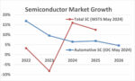
The overall semiconductor market has been weak the last two years after strong pandemic recovery growth of 26% in 2021. According to WSTS, the semiconductor market only grew 3.3% in 2022 and declined 8.2% in 2023. WSTS’ May 2024 forecast was for strong growth of 16.0% in 2024 and 12.5% in 2025. As we stated in our March 2023 newsletter, automotive has been the lone bright spot in the semiconductor market in the last two years. IDC estimated the automotive semiconductor grew 17% in 2022 and 10% in 2023. IDC’s May 2004 forecast called for the growth of the automotive semiconductor market slow to the 5% to 7% range over the next three years.
The combination of slowing production of light vehicles, slower growth of EVs, and delayed deployment of autonomous-driving vehicles will reduce the growth rate of the automotive semiconductor market. The semiconductor industry can no longer count on automotive as a major driver in the next couple of years. However, other sectors are expected to drive growth. Artificial intelligence (AI) is growing rapidly, spurring growth in the computer sector. The memory market has recovered from weak demand and overcapacity. The smartphone market has turned positive in 2024 after declines in 2022 and 2023. Yet the major automotive semiconductor companies are heavily dependent on automotive for the majority or a major portion of their revenues. Thus, they are likely to lag semiconductor industry growth in the next few years.