You are currently viewing SemiWiki as a guest which gives you limited access to the site. To view blog comments and experience other SemiWiki features you must be a registered member. Registration is fast, simple, and absolutely free so please, join our community today!
The first tool company to report Q2-24 results is ASML, and the lithography leader delivered a result above the guidance of EUR5.95B. Revenue of EUR6.242B is 4.9% above guidance and 18% above last quarter’s result of EUR5.29B.
Both operating profit and gross profit grew but not to the level of the end of last year. ASML management calls 2024 a transition year in investor communications, indicating a stronger 2025.
Tool revenue increased after a significant dip. Service Revenue is much more resilient than tool revenue, as it is dependent on the installed base of tools.
Almost all of the tool revenue growth came from memory tool sales, indicating that the memory companies are finally ready to make substantial investments in new capacity, which is much needed after the shift to HBM production.
From a product perspective, the short-term trend of EUV revenue decline continued while the immersion product sales were solid.
Immersion is a technique that utilises that light through water, resulting in amplification, allowing better resolution at the same light wavelength.
Given the Chips Act and other subsidies, the ASML result is somewhat counter-intuitive as EUV is used for 3-7nm leading-edge manufacturing nodes, and immersion is used for 7-14nm. Given the US attempt to become a leading-edge manufacturing location, it could be expected that leading-edge tools would dominate revenue. This indicates that the new factories are not yet in the tooling phase.
The other significant consumer of leading-edge tools is TSMC, which reported Q2-24 result right after ASML.
Although Capex spending was up, it was still just slightly above the maintenance investment level—the investment needed to maintain the deterioration of the existing manufacturing assets. TSMC is likely waiting for ASML’s High-NA tool to be available. ASML has confirmed they shipped one of these babies last quarter and installed another in Veldhoven on the joint IMEC/ASML manufacturing line. The tool is priced North of $350M, and ASML is trying to reach a production capacity of 20 systems annually during the 24/25 timeline.
Despite beating the guidance and reasonable growth, the ASML share price plunged in the stock market. Are the markets losing confidence in the Lithography leader?
What about China?
The key reason for the decline is the ASML result coincided with news that further export limitations are in the works.
Since the signing of the Chips Act, tool sales to China have exploded. While this could be expected, it seems like the US administration’s patience has run out.
The Chinese companies have not had access to the EUV systems since 2019, and the latest embargo, which began on September 23, banned sales of the immersion systems. This makes 80% of ASML’s products (from a revenue perspective) unavailable for Chinese customers.
As ASML has been allowed to ship the backlog, the effect has been delayed, and China still accounted for 49% of all tool sales in Q2-24.
This, however, is about to end abruptly as the Chinese backlog has been depleted.
The ASML backlog now reflects the embargo revenue view, and from now on, the Chinese revenue will fall to 20% of the total from the current level of 49%.
The potential new embargo will impact ASML’s service revenue, which is currently 24% of total revenue. Under a potential new embargo, ASML can lose the ability to service its Chinese customers, which is incredibly important for keeping the tools alive and productive. As the Chinese manufacturing base could deteriorate fast, this could create new opportunities for ASML as mature node capacity would grow outside China.
The longer-term view
With the likely dip in China business and a potential embargo impacting service revenue, investors are starting to panic and run away from ASML. It is worth noting that this is an amazing company founded on a philosophy of long-term cooperation with its suppliers and other stakeholders. Constant innovation drives higher productivity and tool pricing a reaching an alarming (for customers) increasing in price.
While each tool increases productivity, it is still a hefty price if you want to be at the bleeding edge of Semiconductor manufacturing.
The current ASML manufacturing plan will enable the company to deliver a 20B$+ quarter (at current pricing) at the end of 2026. This is not a given or a forecast and can be changed according to industry development. However, it is a very strong indication that the company has faith in the long-term future of the current strategy.
Our research is focused on the business results and not on investment advice. However, if you have faith in the long-term plan of ASML, it might be too early to dump ASML shares.
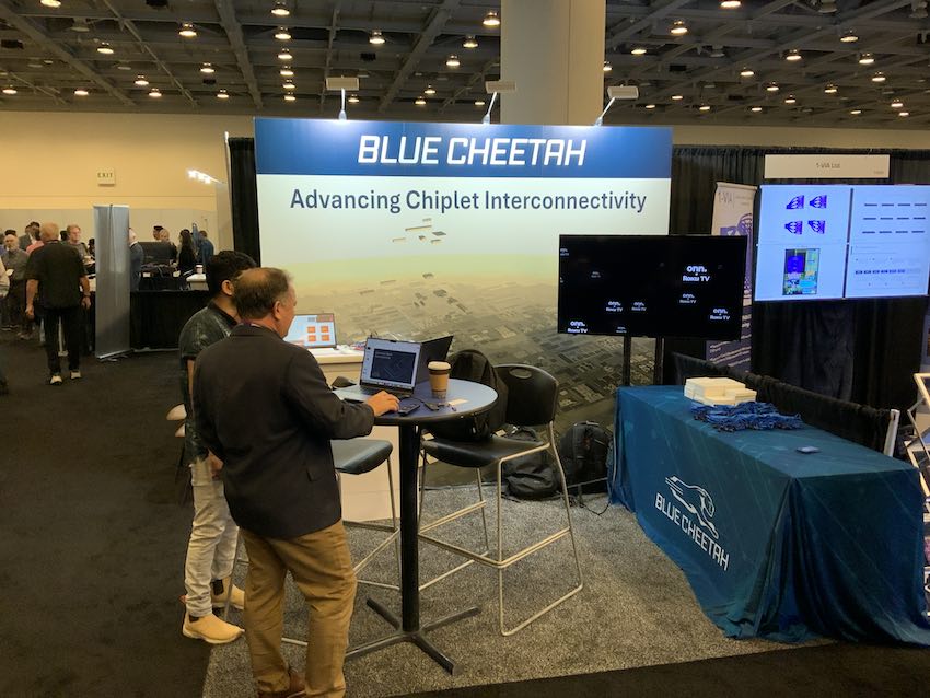
At #61DAC, I love it when an exhibitor booth uses a descriptive tagline to explain what they do, like when the Blue Cheetah booth displayed Advancing Chiplet Interconnectivity. Immediately, I knew that they were an IP provider focusing on chiplets. I learned what sets them apart is how customizable their IP is to support specific physical and system bandwidth requirements, how the interconnect IP is configured for cost-sensitive or high-performance cases, how the energy and performance are optimized from 32 Gb/s down to 8Gb/s and lower, being process-ready at nodes from 16nm to 3nm, and finally having been silicon-proven with reference board designs. I sat down with John Lupienski, VP Product Engineering at Blue Cheetah, to better understand what they were all about. John’s background covers roles at Cadence, Broadcom, and Motorola.
Blue Cheetah at #61DAC
Chiplet designers can opt for an industry-standard interconnect, such as UCIe or BOW, or something custom; Blue Cheetah supports either approach. Blue Cheetah is active with the emerging chiplet standards and is an active participant of both organizations. Smaller IO core area, lower energy per bit, tailor-fit designs are compelling reasons to talk with this IP vendor. The company can customize its IP links per each unique application and deliver solutions using advanced process technologies across multiple foundries and supporting standard and advanced packaging technologies. Its IP has been used in tape-outs for chiplet interconnects ranging from 16nm down to the 4nm node.
During DAC, Baya Systems and Blue Cheetah announced their combined chiplet-optimized Network on Chip (NoC) and Physical Layer (PHY) interconnect IP offerings, making it easier and less risky to design with chiplets. Tenstorrent, announced in February that it uses the Blue Cheetah die-to-die interconnect IP for its AI and RISC-V products. Tenstorrent recently announced that it also uses Baya Systems’ NoC fabric IP.
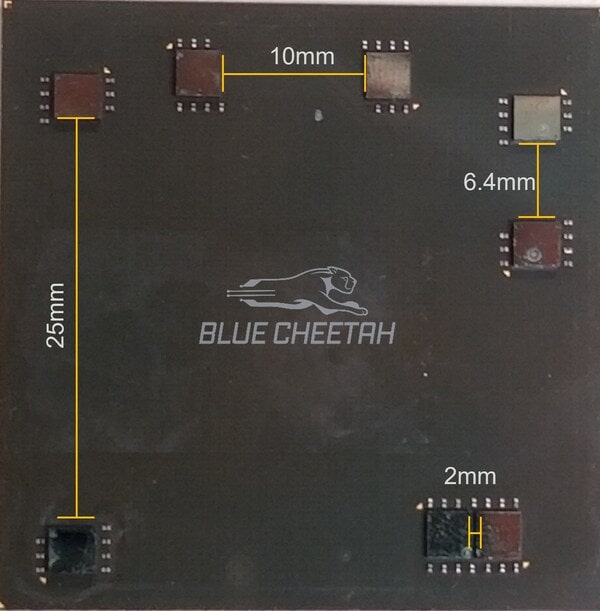
The demonstration at the booth showed test packages integrating 12nm chiplets (availability announced in May 2023) with channel lengths spanning 2mm up to 25mm. Blue Cheetah’s customers’ develop products for a wide variety of end markets; in addition to Tenstorrent, publicly known examples of Blue Cheetah’s customers and partners include DreamBig Semiconductor, FLC, and Ventana Microsystems.
Blue Cheetah test chip, various channel lengths
The architecture of the interconnect IP is modular, making it quicker to port to newer process nodes. John mentioned that packaging for chiplets requires an engineer to perform SI/PI analysis, as customers often use an OSAT to assemble, and each chiplet can be fabricated at different nodes, so you really want interconnect IP that has been silicon-proven. To help get you started with chiplets, they offer reference boards and software to speed up the learning curve.
Summary
SoCs have been around for decades, while the trend of using chiplets has just started in the last several years. Blue Cheetah is a trailblazer in the industry and has solidified its position with high-speed, low-latency, power-efficient D2D BlueLynx™ interface products. The company’s standards-based and customizable IP solutions are available now in 16nm,12nm, 7nm, 6nm, 5nm, 4nm, 3nm, and below across multiple semiconductor foundries.
You can follow up with John directly or contact the company on its website for more info. The company appears at many events throughout the year, including DAC, Chiplet Summit, ISSCC, OCP Global Summit, SemIsreal Expo, and foundry events.
The chip industry got a double tap of both China & Taiwan concerns
Bloomberg reported the potential for draconian China chip restrictions
Trump threw Taiwan under the bus demanding “protection money”
Over-inflated chip stocks had a “rapid unscheduled disassembly”
US looking to further restrict ASML & Tokyo Electron
It has been reported by Bloomberg that the US is going to crack down further on chip equipment sales.
Unfortunately the main targets appear to be non US semiconductor equipment companies such as ASML & Tokyo Electron rather than US equipment companies which sell a similar percentage of their wares to China.
The US government is obviously punishing foreign firms more than US firms, Such as AMAT, LRCX & KLAC that are doing the same thing. Perhaps not wanting to hurt US companies…..or perhaps the government is finally realizing their efforts haven’t worked and will finally crack down on US based sales to China.
We mentioned in our note last week about the tens of millions of dollars being spent lobbying the government on behalf of US equipment companies…..maybe its not enough or the government is finally realizing they need to do more
Foreign Direct Product rule
….says that the US can restrict foreign companies, like ASML & Tokyo Electron from selling and servicing equipment that contains US technology.
ASML famously bought Cymer, a US company in San Diego for their DUV & EUV sources.
Most investors don’t know that Cymer had a lot of “star wars” defense industry technology involving high power lasers and that ASML had to get permission from US defense related officials in order to acquire Cymer. Any agreements ASML made in order to achieve permission were never publicly released, but we would imagine the US government retained some sort of influence
The government is likely as concerned about chip technology as well as high power laser technology
Tokyo Electron does a lot of R&D in the US (as does ASML), so we are sure their products contain US technology in many places….its impossible to avoid
That giant “sucking sound”
We had mentioned in our note last week that US equipment companies would be “sucking major wind” if they lost the 40% plus of their sales which go to China.
But its much worse than it appears on the surface. US chip equipment companies charge Chinese companies a whole lot more than TSMC or Samsung, so the margins are much higher on that 40% plus than of the 50%+ non China sales.
We would not be surprised if closer to 60% or more of profitability comes from China sales. Thus losing China sales has an oversized impact on the bottom line.
US semiconductor equipment companies could actually lose money for the first time in many years if China sales were curtailed enough…..it could get very ugly very fast….
The Mafia “Don” wants “protection money” from Taiwan
Having been born and raised in New York we were very familiar with local establishments paying “protection money” to organized crime types to prevent something bad from happening…….
You can imagine the phone call from the US to Taiwan….” nice little island you got there, you wouldn’t want anything bad to happen to it, would you?”, “cut us in for 20 percent of the action on those chip things you make….”
This scenario is not as far fetched as it would sound as Donald Trump today suggested that the US might not defend Taiwan if they didn’t pay the US for that “protection”….so much for helping out friends and allies….obviously Ukraine will get a similar message.
This statement threw gasoline on an already raging China restriction issue that had the chip stocks in turmoil already.
If the US restricts China sales and China blockades Taiwan at Trumps invitation, equipment sales at the number one and number two markets are at risk……a very bad day…..
The Stocks
…were obviously crushed today on this double whammy of news.
Its not like the stocks were at low valuations to begin with. We have pointed out time and again that the stocks were overheated and over extended. We certainly think AI is the greatest thing in technology ever, but a lot of unrelated chip and chip equipment names got run up in the tsunami.
We will likely see a near term valuation reset across many names in the semi space.
Final valuations and impacts will not truly be known until the US actually publicly states what’s going on and how bad the damage will be. Until then it will be a guessing game but just guessing how bad the impact will be as its all negative.
Initially it will be ASML & TEL but we think this time US companies will likely finally feel some pain as well…..we just don’t know how much it will hurt……
About Semiconductor Advisors LLC
Semiconductor Advisors is an RIA (a Registered Investment Advisor),
specializing in technology companies with particular emphasis on semiconductor and semiconductor equipment companies.
We have been covering the space longer and been involved with more transactions than any other financial professional in the space.
We provide research, consulting and advisory services on strategic and financial matters to both industry participants as well as investors.
We offer expert, intelligent, balanced research and advice. Our opinions are very direct and honest and offer an unbiased view as compared to other sources.
As AI and 5G technologies burgeon, the rise of interconnected devices is reshaping everyday life and driving innovation across industries. This rapid evolution accelerates the transformation of the chip industry, placing higher demands on SoC design. Moore’s Law indicates that while chip sizes shrink, the number of transistors increases rapidly. It is hard to imagine achieving such highly integrated, large-scale designs without advanced EDA tools.
Tape-out is a critical and high-risk phase in chip design. Even a minor error can lead to significant financial losses and missed market opportunities. Logic or functional errors account for nearly 50% of tape-out failures, with design errors comprising 50%-70% of these functional defects. Therefore, verification of SoC design is crucial to successful tape-out. SoC verification is highly complex, taking up about 70% of the entire cycle. To accelerate time-to-market, system software development and pre-tape-out verification must be conducted concurrently, highlighting the significant advantages of prototyping.
For large-scale SoC designs, traditional software simulations often fall short due to the slow execution speed. Consequently, prototyping and hardware simulations have emerged as the primary verification methods, with high-performance prototyping taking the lead. Prototyping, particularly FPGA-based, can be thousands to millions of times faster than software simulations. It is more cost-effective and faster than hardware simulations, making it indispensable for verifying complex SoCs. However, manually built prototyping platforms are difficult to maintain and scale in multi-FPGA and complex design environments. This method is time-consuming and prone to errors, leading to increased risks of project delays and cost overruns. Commercial prototyping solutions have thus emerged to address these challenges.
The Birth of Commercial Prototyping
In 1992, Aptix, the pioneer in the prototyping area, launched the System Explorer system, utilizing FPGAs and custom interconnect chips to achieve commercial prototyping. In subsequent years, projects such as Transmogrifier-l from the University of Toronto, AnyBoard from North Carolina State University, Protozone from Stanford University, and BORG from the University of California, Santa Cruz, explored ways to implement HDL chip designs on prototyping boards. Although these projects were not ready for large-scale commercialization, Aptix’s success inspired other vendors to spark interest in this field. Despite later being absorbed in mergers, Aptix’s pioneering contributions to chip verification methodology remain historically significant.
In 2003, Toshio Nakama founded S2C in San Jose, California, after departing from Aptix. At DAC 2005, S2C unveiled its first prototyping product, the IP Porter, and soon launched the commercially successful Prodigy series. This marked a new era for the company, positioning S2C as a leader in rapid SoC prototyping solutions. Concurrently, the Dini Group in the US released its first commercial FPGA prototyping system, the DN250k10, based on six Xilinx XC4085 FPGAs, providing a flexible and cost-effective solution for design teams. Around the same period, Sweden’s HARDI Electronics AB launched its first FPGA-based prototyping system, HAPS, using Xilinx Virtex FPGAs.
Rapid Growth Driven by Competition
In 2008, Synopsys entered the prototyping market by acquiring Synplicity for $227 million, marking the start of a rapidly growing and competitive era for prototyping. Synopsys spent nearly four years integrating the technology, eventually releasing the HAPS-70 series, a fully automated prototyping product. This acquisition significantly grew the prototyping market, previously dominated by software and hardware simulation tools.
Cadence soon followed suit. Historically focused on designing its FPGA boards, Cadence faced challenges until it acquired Taray in March 2010. Taray’s pioneering routing-aware pin assignment technology optimized FPGA design with the circuit board, aiding in the development of a robust prototyping platform. Cadence later collaborated with the Dini Group to develop the Protium prototyping product. However, Dini Group was acquired by Synopsys on December 5th, 2019. Today, Cadence focuses on streamlining the integration between its prototyping and hardware simulation products, ensuring seamless connectivity.
Siemens EDA (formerly Mentor Graphics acquired in 2016), had a turbulent history in prototyping. In the late 1990s, Siemens EDA licensed emulation technology from Aptix but faced several challenges. To enhance its timing-driven and multi-FPGA partitioning capabilities, Siemens EDA acquired Auspy and Flexras Technologies, the latter known for its “Wasga” automatic partitioning software. In June 2021, Siemens EDA further strengthened its prototyping portfolio by acquiring PRO DESIGN’s proFPGA product series.
The entry of these major companies, along with providers like S2C, facilitated the shift from software and hardware simulation to automated prototyping solutions, enhancing the efficiency and accuracy of SoC designs, and paving the way for further innovations in the entire EDA industry.
Major Challenges and Solutions in Prototyping
The emergence of innovative prototyping solutions has driven increased complexity in SoC design and heightened demands for rigorous prototyping. These solutions require specialized expertise to manage design partitioning, mapping, interface and communications with external environments, debugging, and performance optimization. Consequently, prototyping has become a high-barrier field with only a few EDA companies maintaining a leading position. Some companies even rely on continuous mergers to strengthen their market presence.
As a leader in prototyping, S2C addresses challenges in multi-FPGA RTL logic partitioning, interconnect topology, IO allocation, and high-speed interfaces by timing-driven RTL partitioning algorithms and built-in incremental compilation algorithms. S2C continually updates hardware configurations to support more FPGAs and offer higher-performance connectors ensuring its technology remains at the industry’s forefront.
With over 20+ years of industry experience and a relentless commitment to innovation, S2C equips clients with the highly trusted tools necessary to stay ahead in the competitive market. Their comprehensive solutions accelerate time-to-market, offering unparalleled speed, accuracy, and reliability.
#61DAC was buzzing with discussion of chiplet-based, heterogeneous design. This new design approach opens new opportunities for applications such as AI, autonomous driving and even quantum computing. A critical enabler for all this to work is reliable, cost-effective advanced packaging, and that is the topic of this post. Sarcina Technology is a company focused on delivering reliable, cost-effective advanced packaging through a palette of advanced engineering services. You can learn more about this unique company on SemiWiki here. Let’s see how Sarcina revolutionizes advanced packaging at #61DAC.
The Keysight Connection
As DAC becomes the chips to systems conference, Keysight Technologies becomes more relevant at the show. In its own words, Keysight is your innovation partner, delivering market-leading design, emulation, and test environments that help you develop and deploy faster, with less risk, throughout the product life cycle. Keysight had a partner theater in its booth at #61DAC, and Sarcina’s CEO, Larry Zu was there to explain how Sarcina revolutionizes advanced packaging with Keysight’s help.
The focus of Larry’s presentation was around something called Bump Pitch Transformer package design. A Bump Pitch Transformer for high I/O interconnect density between adjacent dice is a silicon bridge technology that replaces expensive silicon TSV interposers with more cost-effective re-distribution layers (RDL). It’s ideal for homogenous and heterogenous chiplet integration targeting high-performance computing (HPC) devices for AI, data center, microprocessor, and networking applications.
FOCoS B from ASE
Larry explained that Fan-Out Chip-on-Substrate with Silicon Bridge (FOCoS-B) is the latest Bump Pitch Transformer technology. Armed with production-level package design rules and the know-how to design advanced FOCoS-B package with this technology, today Sarcina Technology is ready to design this package for any customers in the world. The manufacture is now available through OSAT companies such as ASE and SPIL, breaking a logjam of innovation created by previous proprietary technologies and essentially democratizing the 2.5D era. The technology transforms silicon micro-bump pitch (~45 microns) to C4 bump pitch (130-150 microns).
Sarcina Technology provides a choice of either silicon bridge (graphic 1a) or chip-last technology (graphic 1b) depending on I/O interconnect density between adjacent dice. FOCoS-B is suitable for higher density and FOCoS-CL (Chip Last) is suitable for lower density. See figure below.
Bump Pitch Transformer Options
While all these advances are exciting, Larry pointed out the complexities design teams will face to reliably and accurately achieve the goal. Challenges include:
Shrinking bump pitch to increase interconnect density
Bump pitch transformer from microbump pitch to C4 bump pitch
Fab or assembly house availability
Design expertise and factory engineering collaboration
Cost effective EDA tools
Bump pitch transformer (interposer) yield and its assembly yield
Cost effective testing
Getting all these right requires substantial engineering talent and a highly accurate simulation and analysis tool flow. This is where Keysight’s PathWave Advanced Design System (ADS) and Memory Designer help quite a bit. Larry explained that the results of these tools have been tuned to be highly accurate. If the simulations look good, one can tape out with confidence.
The Bump Pitch Transformer (BPT) services offered by Sarcina include:
An under-appreciated but critical component in signing off the final stage of chip design for manufacture is timing closure – aligning accurate timing based on final physical implementation with the product specification. Between advanced manufacturing processes and growing design sizes, the most important factors determining timing – interconnect resistance and capacitance parasitics – have become more and more difficult to estimate accurately before final layout. Which is a problem since unexpected variances may require expensive rework at a time when the product schedule calls for speedy transition to manufacturing handoff.
Digital design flows have largely compensated for such variances through further automation and improved virtual modeling of likely interconnect topologies. Following pre-signoff analyses, designers can be reasonably sure that necessary post-layout ECOs, if any, should be relatively limited and easy to fix. Not so in analog (also mixed signal and RF). According to Hao Ji (VP R&D at Cadence, particularly responsible for parasitic extraction) and Akshat Shah (Sr. PE Group Director for the Virtuoso Platform at Cadence), analog design lacks the heavy automation common in digital flows and still depends heavily on handcrafted layouts guided by hand-estimated parasitics. As a result, while earlier generation analog post-layout sims might also have converged quickly, now they never work first time.
This challenge for analog closure is not a minor issue. Surveys indicate that drivers for silicon respins are now dominated by analog issues, not surprising since analog now plays a growing role in almost all large chip-designs – in PCIe, DDR/HBM and Ethernet interfaces, also in sensing. All domains on which modern systems advances critically depend.
Differences between estimated and real extracted parasitics can commonly take 6-8 weeks to diagnose and resolve, at a time when the pressure to tapeout is most intense. To squeeze this time, solutions must accommodate to the unique challenges of analog, helping to accelerate expert designer insight and suggested fixes before starting long-cycle layout changes and re-simulation. That’s what the Cadence QuantusTM Insight Solution offers.
What makes analog post-layout signoff so difficult?
Part of the problem is simply the cycle time to make and re-verify changes: updating the schematic/layout, re-verifying through LVS, then re-verifying through SPICE(or other) simulation. This is a much slower cycle than hand-tweaking a digital netlist and re-running logic simulation, especially since even the fastest modern circuit simulators run 2-3 orders of magnitude slower than a (software) logic simulator.
A circuit designer suggests constraints to guide a layout designer, such as “make this connection no more than 10 ohms”. For the layout designer this advice is an approximate guideline since the complexity of routing through multiple layers and vias makes both resistance and capacitance hard to estimate. The layout designer will do their best, a very short route perhaps, but it won’t match the constraint precisely.
More generally, resistances in an advanced process have become critically important and are very hard to estimate in complex topology nets traversing through multiple layers of interconnect and vias. Field solvers are needed to determine accurate values so it shouldn’t be surprising that back-of-the-envelope calculations may be quite far off. Common fixes to address high resistance paths are known, for example arrayed vias or parallel routing paths. But first you need to know where such fixes might be needed.
Differential pairs present another challenge, in some ways easier to manage in layout because the layout designer knows that such connections must be exactly symmetric. But what isn’t easy to account for is capacitance contributions from neighboring wires, or from metal fills which don’t respect symmetry. Those effects aren’t going to be clear until post-layout extraction.
Diagnosing and determining optimal solutions to such problems depends on the judgement of expert designers. For now at least this judgement can’t be automated away, however automation can simplify debug and trial fixes. This is where the Quantus Insight Solution can help.
The path to diagnosis and what-if experiments
According to Hao, a DSPF extracted from a circuit of 100k instances can run to more than tens of millions of parasitic elements. The DSPF is an ASCII file, clearly at this scale completely unmanageable for manual analysis. Quantus Insight Solution bridges this gap by acting as a visual interactive DSPF debugger, coupled with Virtuoso schematic and layout views.
Suppose you know roughly where to look for a problem. You can zoom in on schematic or layout views to see overlaid resistance, capacitance or estimated (Elmore) delay values for point-to-point connections or layer-wise splits of a net. These are visualized as sorted tables (of R, C or delay), highest values first together with a heatmap representation of corresponding parasitic nets. From this view it’s often quite easy to see why the implemented layout deviates from the spec, for example in an R segment perhaps exceeding the constraint for the whole net, also to see which layer (or via) contributed significantly to that problem.
Sometimes the root cause for an error won’t be quite so obvious; say a differential pair fails to match but there are no standout culprits in either R or C. This is where Elmore delay estimates can be helpful, to highlight cumulative deviations in matching the pair.
If you don’t have a starting point, you can compare with the constraints set to guide layout, or you can compare 2 DSPFs, perhaps one working and one not working, to quickly isolate problem areas. For example if a capacitance is much higher than expected you can see exactly which layer contributed to that excess.
Then you can run a what-if analysis on changes you think may correct a problem. For example, you might change a resistance component and ask to recompute effective resistance to get a first order sense of whether that resolves the issue. If that fix looks good, Quantus Insight Solution can quickly generate a new DSPF on which you can re-run (SPICE) simulation to further verify suitability of the fix. In this way you can iterate relatively quickly through open issues. Only when satisfied do you need to go back to the layout designer to implement your suggested fixes.
Transistor-level circuit designers have long used SPICE for circuit simulation, mostly because it is silicon accurate and helps them to predict the function, timing, power, waveforms, slopes and delays in a cell before fabrication. RTL designers use digital simulators that have a huge capacity but are lacking analog modeling. So, how would you simulate an AMS chip design quickly and accurately?
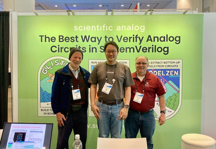
At #61DAC I met with Jaeha Kim, CEO and Founder of Scientific Analog to learn how their approach allows an SoC design and verification team to model Analog circuits in SystemVerilog and UVM by using a plugin called XMODEL. The secret sauce with XMODEL is how it models analog functionality inside of an event-driven simulator.
Charles Dancak, Jaeha Kim, Rafael Betaourt
If you tried to digitize all the points in a continuous analog waveform it would make simulation too slow, instead with XMODEL there are equations that define the analog waveforms, and equations simulate quite fast and accurately. With XMODEL they are propagating analog outputs by using a Laplace transform on s-domains, where the simulator only has to compute something once per output equation.
I asked if XMODEL could be used to simulate something like a PLL, a typical AMS block that simulates very slowly in SPICE. Yes, with XMODEL a PLL can be simulated in SystemVerilog as dozens of pre-built primitives. Engineers would start with their SPICE or Spectre netlist and run the tool to automatically create a SystemVerilog netlist with XMODEL primitives. There are 220 XMODEL primitives to work with, and engineers may add their own XMODEL primitives, or ask Scientific Analog to add a new primitive. You won’t have to learn about writing something new and arcane like Real Number Modeling (RNM) with this XMODEL approach. Digital designers can run full chip AMS designs without being analog modeling experts by using XMODEL in their SystemVerilog and UVM simulations.
Engineers can also visually connect together XMODEL primitives with GLISTER by drawing schematics in Cadence Virtuoso, all without having to code anything. This approach allows you to check out the function of your analog idea before doing any detailed implementation work.
Chiplet design is growing in popularity and there’s an archived webinar on how to do UCIe PHY modeling and simulation with XMODEL at their site, and it goes into an overview of UCIe, an introduction to XMODEL, electrical layer modeling of transmit clock paths, then simulation results. Visitors can even download the slides and model package to get a better idea of how UCIe can be modeled using SystemVerilog.
More than 40 companies and universities are using XMODEL for their AMS design and verification, with names like: Samsung Electronics, Samsung Foundry, SK Hynix, Chinese Academy of Sciences, and Sung Kyun Kwan University. Scientific Analog is a member of the Si2 Open Access Coalition, and Accellera.
Verification engineers with big digital and little analog will greatly benefit from using XMODEL, and design engineers can quickly test out their new ideas before implementation begins. The XMODEL approach is much easier to learn and implement compared to using Verilog-A or Verilog-AMS. Analog designers don’t have to be afraid of learning SystemVerilog and UVM, because with XMODEL and MODELZEN they can quickly create something for their analog cells that can be used by their digital co-workers.
Another powerful use for XMODEL is with silicon photonics, as they process signals at the highest frequencies and using equations is always faster to simulate than digitized points. XMODEL has primitives designed for silicon photonics engineers. In fact, you can now simulate the combination of photonics, analog and digital circuits with XMODEL primitives today in SystemVerilog.
Scientific Analog was at #61DAC in June, DVCon US in February, DVCon Europe in October 2023, and they sponsored ASP-DAC in January 2023.
Summary
My visit with Scientific Analog was a fruitful one, as I learned how their unique technology called XMODEL allows analog modeling and simulation inside of SystemVerilog and UVM. The company has been around since 2015 and was founded in Palo Alto, CA, and now has distributors in Japan, China and North America. If you’re a design team doing AMS photonic designs, then I would give Scientific Analog a closer look for modeling, simulation and verification tasks.
PCIe design complexity continues rising as the standard for intrasystem communication evolves. An urgent need for more system bandwidth drives PCIe interconnects to multi-lane, multi-link, multi-level signaling. Classical PCIe design workflows leave designers with most of the responsibility for getting the requisite interconnect details right. These classical workflows also defer compliance testing until physical realization – when it can be too late to fix unforeseen chip problems. Keysight is revamping the PCIe design workflow with smart workflow automation in System Designer for PCIe®, including IBIS-AMI model generation and simulation-driven virtual compliance, speeding design cycles and reducing risk in a shift-left approach. We discussed the technology with Hee-Soo Lee, Director of High-Speed Digital Segment at Keysight.
Replacing tedious setups and hard debugging with workflow automation
Traditional high-speed digital design requires PCIe designers to complete tedious manual design setups. In the example below, designers face a choice of whether to use a retimer (RT) and where to place it in the signal chain between the root complex (RC) and the endpoint (EP). Many scenarios benefit from using an RT, introducing two schematics, one between the RC and RT and another between the RT and EP, requiring individually wired signal connections from S-parameter blocks to signal drivers. Creating all the connections for complex multi-lane, multi-link designs can be very tedious.
Classical PCIe design workflow adding a retimer with two schematics
Parameter sweeps in conventional high-speed digital simulations span many points, resulting in large data sets, and gathering insights becomes time-consuming. If eye diagrams from the analysis are closed, debugging channel performance is the first step, but it becomes a problem as the connections around the S-parameter blocks must be unwired and manually terminated for further simulation. Measurement probes also require manual insertion. Any mishaps in wiring or unwiring signals and terminations inject errors into debugging, requiring more investigation. If manual tasks like these become automated, designers can spend more time optimizing designs.
Lee contrasts this classical approach with the smart PCIe design workflow using Keysight’s Advanced Design System (ADS) and System Designer for PCIe®. “One schematic implements a topology with the RootComplex and EndPoint placed as smart components,” he says. “Smart bus wire makes all the connections accurately, automated with a click.” Below is the System Designer for PCIe® representation of Topology 3 above. Automatic placement of PCIe probes simplifies multi-dimensional data capture using smart measurement technology. What once consisted of hours of work in layout is now a few minutes, and preparing for and running a PCIe simulation is a few seconds.
Smart components for the same PCIe retimer placed in System Designer for PCIe®
Control over parameters and choice of simulations in one interface
Each of these blocks is configurable in the System Designer for PCIe® user interface. Expanding the example above to look at the PCIe Mid-Channel Repeater block shows some options. Designers can choose whether the block is a redriver or retimer, select how many differential pairs are in the link, and select an IBIS file for the model. Smart wire makes the connections with the correct parameters automatically. Designers can also set up bit-level system behaviors.
PCIe mid-channel repeater with configuration parameters
Simulation options from one schematic with no manual conversions also give control over the PCIe design workflow. Most PCIe designers are already familiar with Seasim, the statistical simulator from the PCI-SIG, which guides PCIe compliance evaluation. Existing workflows required designers to jump from their preferred simulation tool to the Seasim environment. When choosing Seasim simulation mode in System Designer for PCIe®, ADS characterizes the channels using its S-parameter simulator and launches Seasim (user-installed separately) from ADS for analysis.
Seasim interface in System Designer for PCIe®
In addition to the S-parameter simulator and the Seasim interface, two other simulation methods are available for selection in System Designer for PCIe®:
A bit-by-bit simulator exercises sequences of bits specified in transmitters for durations specified in analysis settings, which helps analyze systems faster with waveform information embedded.
A statistical simulator uses ADS proprietary algorithms to analyze random and periodic jitter, duty-cycle distortion, and other effects to achieve an extremely low bit error rate (BER).
IBIS-AMI modeling and virtual compliance evaluation
IBIS-AMI behavioral modeling for SerDes transceivers captures analog characteristics and algorithmic functionality such as equalization, gain, and clock data recovery. Millions of bits through a link can be simulated using convolution and data flow approaches in a few minutes.
Usually, a designer must have intimate knowledge of digital signal processing details and C coding to create an AMI model. With the PCIe AMI Modeler in System Designer for PCIe®, AMI model generation has become a simple task in the wizard-driven AMI modeling workflow. This capability is essential for cutting-edge PCIe Gen6 designs with multi-level PAM4 signaling, where AMI models may not exist yet. Output files include .dll for Windows or .so for Linux.
PCIe AMI Modeler in System Designer for PCIe®
Finally, System Designer for PCIe® adds simulation-driven compliance. “Typically, PCIe compliance tests are done in the physical realm, using a detailed Method of Implementation in an oscilloscope application, testing performance against compliance metrics,” says Lee. “The problem is this is very late in the design cycle to discover for the first time if compliance tests pass or fail, and the risks are huge in complex designs.”
A guiding principle for Keysight EDA is using unified measurement science proven from hardware verifications in simulation-driven tests. The software that powers Keysight test equipment also runs in the Keysight EDA design environment – same algorithms, same methodologies. System Designer for PCIe® carries that principle to PCIe compliance testing with a specialized PCI Compliance Probe that sets up the correct stimulus and makes the appropriate compliance measurements. Users can accurately and thoroughly gauge PCIe design compliance from early-stage designs before committing to hardware.
This smart PCIe design workflow slashes the design cycle while providing faster insight into performance and a much earlier look at compliance. Keysight EDA is offering a deeper dive into System Designer for PCIe® and its capabilities in a webinar – registration is now open.
Part 1 of this 4-part series introduces the complexities of developing and bringing up the entire software stack on a System on Chip (SoC) or Multi-die system. It explores various approaches to deployment, highlighting their specific objectives and the unique challenges they address.
Introduction
As the saying goes, it’s tough to make predictions, especially about the future. Yet, among the fog of uncertainty, a rare prescient vision in the realm of technology stands out. In 2011, venture capital investor Marc Andreessen crafted an opinion piece for The Wall Street Journal titled “Why Software Is Eating The World.” Andreessen observed that the internet’s widespread adoption took roughly a decade to truly blossom, and predicted that software would follow a similar trajectory, revolutionizing the entire human experience within ten years.
His foresight proved remarkably accurate. In the decade following Andreessen’s article, software’s transformative power swept through established industries, leaving a lasting impact. From industrial and agricultural sectors to finance, medicine, entertainment, retail, healthcare, education, and even defense, software reshaped landscapes disrupted traditional models. Those slow to adapt faced obsolescence. Indeed, software has been eating the world.
This rapid software expansion lies at the core of the challenges in developing and delivering fully validated software for modern SoC designs.
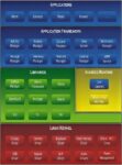
The Software Stack in a Modern SoC Design
In a modern System on Chip (SoC) the software is structured as a software stack that consists of several layers, each serving specific purposes to ensure efficient operation and functionality:
1) Bare Metal Software and Firmware:
Bare Metal Software: Specialized programs that run directly on the hardware without an underlying operating system (OS) into memory upon startup. This software interacts directly with the hardware components.
Firmware: Low-level software that initializes hardware components and provides an interface for higher-level software. It is critical for the initial boot process and hardware management.
2) Operating System (OS):
The OS is the core software layer that manages hardware resources and provides services to application software.
3) Middleware:
Middleware provides common services and capabilities to applications beyond those offered by the OS. It includes libraries and frameworks for communication, data management, device management, dedicated security components such as secure boot, cryptographic libraries, and trusted execution environments (TEEs) to protect against unauthorized access and tampering.
4) Drivers and HAL (Hardware Abstraction Layer):
Device Drivers: These are specific to each hardware component, enabling the OS and applications to interact with hardware peripherals like GPUs, USB controllers, and sensors.
HAL: Provides a uniform interface for hardware access, isolating the upper layers of the software stack from hardware-specific details. This abstraction allows for easier portability across different hardware platforms.
5) Application Layer:
This top layer consists of the end-user applications and services that perform the actual functions for which the SoC is designed. Applications might include user interfaces, data processing software, and custom applications tailored to specific tasks.
Figure 1 captures the structure of the most frequently used software stack in modern SoC design.
Figure 1: Example of Android Software Stack, Source: researchgate.ne
The Software Development Landscape
The global software development community, estimated to comprise around 12 million professional developers, is responsible for an astounding amount of code production. Various sources suggest an annual output ranging between 100 and 120 billion lines of code. This vast quantity reflects the ever-growing demand for software in diverse industries and applications.
However, this impressive volume comes with a significant challenge: the inherent presence of errors in new code. Web sources report a current error rate for new software code before debugging ranging from 15 to 50 errors per 1,000 lines. This translates to an estimated average of over 10 billion errors that need to be identified and fixed before software reaches the market. (See Appendix).
It’s no surprise that design verification and validation consume a disproportionately large portion of the project schedule. Tracking and eliminating bugs is a monumental task, particularly when software debugging is added to the hardware debugging process. According to a 2022 analysis by IBS, the cost of software validation in semiconductor and system design is double that of hardware verification, even before accounting for the cost of software development of end-user applications, see figure 2.
Figure 2: Total cost of mainstream designs by process technology node, segmented by design stages Source: IBS, July 2022
This disparity underscores the increasing complexity and critical importance of thorough software validation in modern SoC development.
SoC Software Verification and Validation Challenges
The multi-layered software stack driving today’s SoC designs cannot be effectively validated with one-size-fits-all approach. This complex task demands a diverse set of tools and methods sharing a common foundation: executing vast amounts of verification cycles, even for debugging bare-metal software, the smallest software block.
Given the iterative nature of debugging, which involves running repeatedly tens or hundreds of times the same software tasks, even basic tasks can quickly consume millions of cycles. The issue becomes more severe when booting operating systems and running large application-specific workloads, potentially requiring trillions of cycles.
1) Bare-metal Software and Drivers Verification
At the bottom of the stack, verifying bare-metal software and drives requires the ability to track the execution and interaction of the software code with the underlying hardware. Access to processor registers is crucial for this task. Traditionally, this is achieved using the JTAG connection to the processor embedded in the design-under-test (DUT), which is available for a test board accommodating the SoC.
2) OS Booting
As the task moves up the stack, next comes booting the operating system. Likewise debugging drivers, it is essential to have visibility into the hardware. The demand for verification cycles now jumps to hundreds of billions of verification cycles.
3) Software Application Validation
At the top of the stack sits the debugging of application software workloads with the needs to execute trillions of cycles.
These scenarios defeat traditional hardware-description-language-based (HDL) simulators, as they fall short of meeting the demand. They run out of steam when processing designs or design blocks in the ballpark of one hundred million gates. A major processor firm reported that their leading-edge HDL simulator could only achieve clock rates of less than one hertz under such conditions. This makes HDL simulators impractical for real-world development cycles.
The alternative is to adopt either hardware-assisted verification (HAV) platforms or virtual prototypes that operate at a higher level of abstraction than RTL.
Virtual prototypes can provide an early start before RTL reaches maturity. This adoption drove the shift-left verification methodology. See Part 3 of this series.
Once RTL is stable enough and the necessary hardware blocks or sub-systems for software development are available, HAV engines tackle the challenge by delivering the necessary throughput to effectively verify OS and software workloads.
Hardware-assisted Verification as the Foundation of SoC Verification and Validation
HAV platforms encompass both emulators and FPGA prototypes, each serving distinct purposes. Emulators are generally employed for software bring-up of existing software stacks or minor modifications of software for new SoC architectures, such as driver adaptations. In contrast, FPGA prototypes, due to their substantially higher performance—roughly 10 times faster than emulators—are advantageous for software development requiring higher fidelity hardware models at increased speeds. To remain cost-effective, FPGA prototypes often involve partial SoC prototyping, allowing for the replication of prototypes across entire teams.
Working in parallel, hardware designers and software developers can significantly accelerate the development process. Emulation allows hardware teams to verify that bare-metal software, firmware, and OS programming interact correctly with the underlying hardware. FPGA prototypes enable software teams to quickly validate application software workloads when hardware design visibility for debugging is not critical. Increasingly, customers are extending the portion of the design being prototyped to the full design as software applications require interaction with many parts of the design. The scalability of prototypes into realms previously reserved for emulators is now essential.
Hardware engineers can realize the benefits of running software on hardware emulation, too. When actual application software is run on hardware for the first time, it almost always exposes hardware bugs missed by the most thorough verification methodologies. Running software early exposes these bugs when they can be addressed easily and inexpensively.
This parallel workflow can lead to a more efficient and streamlined development process, reducing overall time-to-market and improving product quality.
Conclusion
Inadequately tested hardware designs inevitably lead to respins, which increase design costs, delay the progression from netlist to layout, and ultimately push back time-to-market targets, severely impacting revenue streams.
Even more dramatic consequences arise from late-stage testing of embedded software, which can result in missed market windows and significant financial losses.
RISC-V continued to be a significant force at #61DAC. There were many events that focused on its application in a wide variety of markets. As anyone who has used an embedded processor knows, the trick is how to be competitive. Using the same core as everyone else and differentiating in software is a strategy that tends to run out of gas quickly. There is simply not enough capability to differentiate in software alone. And so, customizing the processor core becomes the next step. The open-source ISA offered by RISC-V makes it a popular choice for customization. Achieving this goal is easier said than done, however. There are many moving parts to manage, and many pitfalls to be avoided. Codasip has substantial expertise in this area and a newly announced, safer and more robust approach to the problem was on display at DAC. Let’s examine how Codasip makes it easier and safer to design custom RISC-V processors.
Codasip Company Mission
Codasip is a processor solutions company which uniquely helps developers differentiate products. It was founded in 2014, and a year later offered the first commercial RISC-V core and co-founded RISC-V International. The company’s philosophy includes the belief that processor customization is something the end user wants to control. This is the most potent way to differentiate in the market.
Achieving that result requires a holistic approach. This is accomplished through the combination of the open RISC-V ISA, Codasip Studio processor design automation, and high-quality processor IP. Codasip’s custom compute enables its customers to take control of their destiny.
What’s New – A Conversation from the Show Floor
I had the opportunity to meet with two senior executives at the Codasip DAC booth – Brett Cline, Chief Commercial Officer and Zdeněk Přikryl, Chief Technology Officer. I’ve known Brett for a long time, dating back to his days at Forte Design Systems. These two gentlemen cover the complete spectrum of all things at Codasip, so we had a far-reaching and enjoyable discussion. Along the way, we may have uncovered a way to solve most of the world’s problems, but I’ll save that for another post. Let’s focus on how Codasip makes it easier and safer to design custom RISC-V processors.
We first discussed a new version of Codasip Studio called Studio Fusion, which has a capability called Custom Bounded Instructions, or CBI. Using CBI, customers can develop any type of customization needed for their intended market, but by staying within the guidelines of CBI they can be assured the changes will not cause processor exceptions. Essentially, you can’t “break” the processor if you follow CBI.
Anyone who has developed custom instructions knows this is not the case in general and great care must be taken not to introduce subtle, hard-to-find bugs. There is substantial re-verification required. All that goes away with CBI.
We also discussed how limiting this new approach could be. It turns out the answer is “not much”. Significant customization can be accomplished with much lower development time and risk. To drive home that point, Codasip was running a live demo in its booth using a customized processor that was implemented with Codasip Studio Fusion and CBI.
The application applied AI algorithms to analyze the sound of a running cooling fan to identify anomalies in the sound that indicate potential problems. The algorithm would then predict the time to failure for the fan. If the application was cooling for critical electronics or automotive operation, the benefits are clear. After implementing and verifying the code, a custom processor was implemented with 40 unique custom instructions to enhance the performance of the algorithm.
Speed and energy efficiency showed dramatic improvements, with power reduction in the neighborhood of 80 percent. That makes the application much easier to implement in a small, low power form factor. I should also mention that doing a live demo of custom hardware at a trade show requires a lot of confidence – my experience is that all failures find a way forward while folks are watching. This made the demo more impressive in my eyes.
It was also pointed out that Codasip generates all the infrastructure to use the new custom processor, including the compiler and debugger. You get everything required. No third-party tools or support needed. This means no code changes to use the custom processor, the compiler takes care of exploiting the new features. Here, we discussed another new feature that has been added. The compiler is now more micro-architecturally aware. This means the compiler has deeper knowledge of what’s going on in the custom processor and so it can perform more sophisticated and higher-impact optimization.
After my discussion with Brett and Zdeněk it became clear how much automation Codasip is delivering to the RISC-V customization process. You truly are limited only by your imagination.


