Bronco Webinar 800x100 1

Costello on Communicating a Compelling Company Story

Costello on Communicating a Compelling Company Story
by Paul McLellan on 03-14-2013 at 11:53 pm

The next EDAC sponsored emerging company series (what I’ve been calling Hogan University) is Joe Costello being interviewed on how to communicate a compelling company story. Anyone who saw Joe’s keynote at DAC several years ago will not want to miss this. I can’t promise that he’ll lie down on the stage and pretend to be a fish again, but I’m sure it will be interesting.

I’ll tell you his rules from that keynote:

[LIST=1]

  • “Think like a fish.” Know what your customers really want and give it to them.
  • “Write the press release first.” It never gets better than the press release so try and develop your product to measure up to the press release.
  • “Change the rules.” The company that sets the rules wins.

    This will take place at 6pm on May 1st on the Cadence campus (building 10). If you don’t know where the Cadence campus is (you probably worked there at some point, Joe of course did) you surely aren’t in EDA. The event is sure to sell out (it is free, so that “sell” is not quite the right term, but you do need to register).

    Details are on the EDAC website here, including a link for registration.


  • IJTAG for IP Test: a free seminar

    IJTAG for IP Test: a free seminar
    by Beth Martin on 03-14-2013 at 1:53 pm

    What: Better IP Test with IJTAG
    When: 26 March, 2013, 10:30am-1:30pm
    Where: Mentor Graphics, 46871 Bayside Parkway, Fremont, CA 94538


    If you are involved in IC test*, you’ve probably heard about the IEEE P1687 standard, called IJTAG for ‘internal’ JTAG. IJTAG defines a standard for embedded IP that includes simple portable descriptions that can be supplied with the IP itself. This creates an environment for plug-and-play integration, access, test, and pattern reuse of embedded IP that doesn’t currently exist.

    It’s the first new standard designed specifically to deal with the growing amount of IP used in today’s complex designs, and I expect that it will see wide adoption in the industry.

    This seminar from Mentor Graphics covers the key aspects of IJTAG, including how it simplifies the design setup and test integration task at the die, stacked die, and system level. You will also learn about IP-level pattern reuse and IP access with IJTAG. Are you wondering what you need to do to migrate your existing 1149.1-based approach to P1687? Yep, that’s covered in the seminar too.

    Mentor offers a product, Tessent IJTAG, to automate some aspects of implementing P1687, which is described in the seminar. Tessent IJTAG automates design and test tasks, and reduces the length of an aggregated test sequence for all the IP blocks in an SOC. This translates directly into faster production test readiness, reduced test time, and smaller tester memory requirements.

    All the examples used in the seminar are from actual industrial use cases (from NXP and AMD). The presenter is Dr. Martin Keim. He has the experience and technical chops to make this a very useful day for everyone involved.

    Register now!

    *DFT managers, DFT engineers, DFT architects, DFT methodologist, IP-, Chip-, System-Design managers and engineers, IP-, Chip-, System-Test integrator, Failure analysis managers and engineers, system test managers, and system test engineers. Whew!


    ARM Cortex SoC Prototyping Platform for Industrial Applications

    ARM Cortex SoC Prototyping Platform for Industrial Applications
    by Daniel Payne on 03-14-2013 at 1:00 pm

    If your next SoC uses an ARM Cortex-A9 and has an industrial application, then you can save much design and debug time by using a prototyping platform. The price to prototype is quite affordable, and the methodology has a short learning curve. Bill Tomasan Aldec Research Engineer conducted a webinar today on: ARM Cortex SoC Prototyping Platform for Industrial Applications.


    Bill Tomas, Aldec
    Continue reading “ARM Cortex SoC Prototyping Platform for Industrial Applications”


    Synopsys ♥ TSMC!

    Synopsys ♥ TSMC!
    by Daniel Nenni on 03-14-2013 at 8:00 am

    Dr. Paul McLellan and I will be covering the Silicon Valley SNUG live again this year. Unfortunately we are only allowed to see the keynotes (same thing with CDNLive) but they look very good:

    Keynote Address: Massive Innovation and Collaboration into the “GigaScale” Age!
    Aart de Geus, Chairman and co-CEO, Synopsys, Inc.

    The semiconductor industry is on the bridge to a new world of complexity empowered by smaller dimensions, new transistor types, enormous IP reuse, and a focus on the great potential of electronic systems. In other words, the GigaScale Age is upon us! In addition, our customers are facing uncertain markets where merely making a better version of their last product is not sufficient. To survive and thrive in new and unknown markets, designers and their ecosystem partners are accelerating both their innovation and their collaboration with key partners. They expect the same from their EDA, IP and services partners. In his presentation, Aart will give an overview of the enormous amount of recent innovation and collaboration happening at Synopsys as we enable “Moore’s Law plus, plus” for yet another decade!

    Technology Keynote – “From Crystal Ball to Reality — The impact of Silicon IP on SoC Design”
    Sir Hossein Yassaie, PhD, Chief Executive Officer, Imagination Technologies Group

    SoCs have transformed the semiconductor and electronics industries, integrating staggering breadth of functionality and performance into highly cost-effective, low power but complex single-chip solution platforms. However, there has been another transformation: many of the major functional blocks on today’s SoCs are provided by Silicon IP providers rather than designed in-house. Hossein will review some of the important technological and market trends in key segments and discuss how the IP industry is helping to create the ability to translate vision into reality , and to constantly enhance it. He will touch on key functional blocks in modern SoCs explaining how the GPU is becoming the new driving force not only for modern applications but also for design methodologies and process technologies, and how heterogeneous processing is transforming the way SoCs handle key user applications such as UI’s, gaming, multimedia and more.

    Technology Keynote – “Collaborate to Innovate – A Foundry’s Perspective on Ecosystem
    Dr. Cliff Hou, Vice President, Research & Development, TSMC

    Ecosystem refers to a symbiotic, co-dependent, co-evolutionary and multiplicative relationship among its constituents. The semiconductor industry represents one of the largest business ecosystems in the world where the collective diversity and creativity has fundamentally reshaped the human society. As process scaling continues toward the atomic level, challenges abound and stakes are never higher. In this talk, we will offer a foundry perspective of the semiconductor ecosystem and how, through close collaboration, we combine individual specialties and resources to innovate and move the industry forward. Specifically, we will discuss how the collaboration with EDA is becoming ever closer, earlier and wider to enable designs concurrently with process development, even especially at the advanced nodes.

    SNUG Around the world:
    [TABLE]
    |-
    | Silicon Valley
    | March 25-27, 2013
    |-
    | Boston
    | September 12, 2013
    |-
    | Austin
    | September 18, 2013
    |-
    | Canada
    | October 1, 2013
    |-
    | Germany
    | May 14, 2013
    |-
    | United Kingdom
    | May 16, 2013
    |-
    | France
    | June 11, 2013
    |-
    | Israel
    | June 18, 2013
    |-
    | India
    | June 12-13, 2013
    |-
    | Japan
    | July 12, 2013
    |-
    | China
    | August 22, 2013
    |-
    | Taiwan
    | August 20-21, 2013
    |-
    | Singapore
    | August 16, 2013
    |-

    As I mentioned in my blog Synopsys ♥ FinFETs, Synopsys knows FinFETs so be sure to see the FinFET tracks. Paul and I also get to attend the press lunch and hopefully, like last year, an hour roundtable with Aart. It is a great experience to hang with semiconductor people wearing SemiWiki shirts and to get recognized and even photographed. My wife rolls her eyes when it happens and makes me take out the trash when I get home to keep me grounded. But seriously, we all appreciate your support and encouragement and it is a pleasure to collaborate with you.

    Note: TSMC’s Dr. Cliff Hou gets a coveted keynote so clearly Synopsys loves TSMC! Cliff would be a great addition to the Synopsys board dontcha think? I will see what I can do…..

    Since 1991, SNUG (the Synopsys Users Group) has represented a global design community focused on accelerating innovation. Today, as the electronics industry’s largest user conference, SNUG brings together nearly 9,000 Synopsys tool and technology users across North America, Europe, Asia and Japan. In addition to peer-reviewed technical papers and insightful keynotes from industry leaders, SNUG provides a unique opportunity to connect with Synopsys executives, Synopsys design ecosystem partners and members of your local design community. Join your fellow engineers at the SNUG in your region — you’ll leave with practical information you can use on your current projects and the inspiration to accelerate innovation.


    Will next generation Mobile Devices support PCI Express? M-PCIe is coming fast!

    Will next generation Mobile Devices support PCI Express? M-PCIe is coming fast!
    by Eric Esteve on 03-14-2013 at 6:22 am

    Those who have read the numerous articles I have written about MIPI, or PCIe, or the fusion of both named “Mobile Express” know my position: the question is not “Will Mobile devices support PCI Express?” but “When will we see Mobile devices integrating Mobile Express?” I was not really surprised by the Press Release that Cadence has launched yesterday (07 March 2013), claiming the company support for Mobile PCIe Express (M-PCIe) solution, made of MIPI M-PHY IP, PCIe Controller IP and Verification IP for both, as MIPI M-PHY IP was part of Cosmic Circuit port-folio.

    The surprise comes from the fast turnaround time between Cosmic Circuit acquisition and this announcement of M-PCIe support: exactly one month! If, like me, you hate the management posture which is to discuss forever before taking a decision, in fact discuss for such a long time that when the decision is taken it’s too late to get the entire benefit from the decision, you will appreciate this fast move, too!

    What exactly is Mobile Express specification? Just like extracting the best from the two protocols. PCI Express is a very complete (and complex) point to point interface protocol, offering many features (see at the bottom of this article for PCIe feature list) allowing optimizing chip to chip communication in various applications, but with a physical layer tending to be power hungry, when MIPI M-PHY has been specifically defined for mobile devices, targeting low power operation. According with Al Yanes, Chairman and President, PCI-SIG, “M-PCIe brings the necessary architecture to support advancement in tablets and smartphones as they take on the role of primary computing devices. The Mobile market is rapidly evolving and so are consumer expectations, placing an emphasis on low-power with increased performance for a better user experience.”

    In fact, M-PCIe will allow chip makers and system developers, strong in PC segment, to re-use existing PCIe related architecture when moving to the various mobile segments. And MIPI Alliance clearly welcome PCIe related innovation: “The M-PCIe specification provides the Mobile industry with decades of innovation in PCIe technology coupled with the proven M-PHY physical layer that meets low-power requirements needed for today’s mobile device platforms,” said Joel Huloux, Chairman of the Board, MIPI Alliance.

    Existing PCIe Controller IP and Verification IP products and Cosmic Circuits acquisition allows cadence to bring a complete, integrated M-PCIe solution:

    • MIPI M-PHY IP
    • PCIe gen-3 Controller IP
    • Verification IP for both M-PHY and PCIe controller

    The readers familiar with the Interface IP market know that IP vendors able to support both pieces (Controller and PHY) get a competitive advantage over the competition: interoperability between these two parts has been validated by the vendor, and, for the buyer, the acquisition process is easier as he needs to interface with only one supplier, as well is the integration into the chip as the technical support comes from one source. And the same supplier providing Verification IP is also seen as a benefit, from the same reasons.

    Because this announcement is very fresh, we don’t know yet what will be the operating frequency of M-PCIe solution which could be implemented today: PCIe gen-3 link operating frequency is specified at 8 Gbps, when M-PHY gear 3 specifications is 6 Gbps, which lead to an effective data rate of 4.8 Gbps due to 8B/10B encoding…

    No doubt that we can rely on the cumulated energy of the MIPI Alliance contributor members to quickly figure out the best way using M-PCIe. I will let Joel Huloux, Chairman of the Board, MIPI Alliance, to conclude: “Mobile device users demand ever increasing power-efficiency and the MIPI Alliance chip-to-chip interfaces are an essential low power technology for smartphone and tablet developers. As an early contributing member of the MIPI Alliance, Cadence has helped speed the adoption of mobile specifications, now including the M-PHY-based M-PCIe”.

    By Eric Esteve from IPNEST

    Features
    The PCIe core includes these features:

    Single-Root I/O Virtualization
    The PCIe core provides a Gen 3 16-lane architecture in full support of the latest Address Translation Service (ATS) specification, Single-Root I/O Virtualization (SR-IOV) specification, including Internal Error Reporting, ID Based Ordering, TLP Processing Hints (TPH), Optimized Buffer Flush/Fill (OBFF), Atomic Operations, Re-Sizable BAR, Extended TAG Enable, Dynamic Power Allocation (DPA, and Latency Tolerance Reporting (LTR). SR-IOV is an optional capability that can be used with PCIe 1.1, 2.0, and 3.0 configurations.

    Dual-mode operation
    Each instance of the core can be configured as an Endpoint (EP) or Root Complex (RC).

    Power management
    The core supports PCIe link power states L0, L0s and L1 with only the main power. With auxiliary power, it can support L2 and L3 states.

    Interrupt support
    The core supports all the three options for implementing interrupts in a PCIe device: Legacy, MSI and MSIx modes. In the Legacy mode, it communicates the assertion and de-assertion of interrupt conditions on the link using Assert and De-assert messages. In the MSI mode, the core signals interrupts by sending MSI messages upon the occurrence of interrupt conditions. In this mode, the core supports up to 32 interrupt vectors per function, with per-vector masking. Finally, in the MSI-X mode, the controller supports up to 2048 distinct interrupt vectors per function with per-vector masking.

    Credit Management
    The core performs all the link-layer credit management functions defined in the PCIe specifications. All credit parameters are configurable.

    Configurable Flow-Control Updates
    The core allows flow control updates from its receive side to be scheduled in a flexible manner, thus enabling the user to make tradeoffs between credit update frequency and its bandwidth overhead. Configurable registers control the scheduling of flow-control update DLLPs.

    Replay Buffer
    The Controller IP incorporates fully configurable link-layer reply buffers for each link designed for low latency and area. The core can maintain replay state for a configurable number of outstanding packets.

    Host Interface
    The datapath on the host interface is configurable to be 32, 64, 128 or 256-bits. It may be AXI or Host Application Layer (HAL) interface.



    Formal Verification of Power Intent

    Formal Verification of Power Intent
    by Paul McLellan on 03-13-2013 at 4:10 pm

    I can’t imagine that any SoC today is designed without taking intense interest in how much power the chip will consume, whether it is destined for a mobile phone or tethered in a cloud datacenter. One challenge with power is that adding features like voltage islands or power-down areas require changes to the netlist such as adding level-shifters or isolation cells.

    A few years ago, two consortia developed the UPF and CPF power standards that make the power policy orthogonal with the functionality captured in the RTL/netlist. To add a voltage island does not require trawling through potentially large numbers of RTL files adding all the required level shifters explicity, and then, if we change our mind, going through and taking them all out again. Instead, the CPF/UPF file identifies which library elements are level shifters, where the voltage islands are, and so forth. Every EDA tool which reads the RTL/netlist needs to make the same changes to the netlist (level shifters affect timing, for example) whether a simulator, static timing, place and route and so on.

    So the typical development methodology today is to use IP blocks and assemble the RTL for the complete SoC and get the functionality correct. As the design proceeds, the power policy can develop and various power optimizations such as clock shutoff, power shutoff or voltage islands can be added.

    Of course, this leads to a new verification problem. It is no longer good enough to use formal techniques on the netlist alone, there are potentially errors in the way that the way the power policy has been implemented. It is typically not possible to decide the entire power policy ahead of time, it has to develop along with the floorplan since you can’t power down a block, for example, without it being an identifiable area on the floorplan with its own power grid. Plus, of course, there needs to be circuitry added to added to control shutting down and re-starting the block.

    Normal design functionality should not be affected by the addition of the domains and the control registers. Before and after checking is necessary to ensure this. At the end of a power switching sequence the signals should all be generated correctly (with no additional unknowns). Switching off a power domain should not break connectivity between IP blocks.

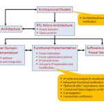
    The RTL before addition of power policy is a golden reference model. Power-aware verification requires a mix of architecture level verification, IP white box functional verification and analysis, exhaustive functional verification, sequential equivalence checking, control/status register verification, X-propagation analysis and connectivity checking.

    Traditional power-aware verification relies on a mix of simulation and rule-checking. Typically problems are corner cases and, of course, these are just the areas where formal techniques tend to excel over simulation based verification.


    The JasperGold Low-Power Verification (LPV) App automatically creates power-aware transformations and automatically generates a power-aware model that identifies power domains, the power supply network and switches, isolation rules and data retention rules. It does so by parsing and extracting relevant data from the UPF/CPF specification, RTL code and user-defined assertions. It then generates assertions that other Apps can use to verify that the power management circuitry does indeed conform to the UPF/CPF specification and does not corrupt the original RTL behavior.

    The JasperGold LPV App is described in more detail in a new Jasper white paper Formal Verification of Power-Aware Designs Using the JasperGold Low-Power Verification App available here.

    Related Blog


    Margaret Butler: One Woman’s Life in Science

    Margaret Butler: One Woman’s Life in Science
    by Holly Stump on 03-13-2013 at 4:00 pm

    46 years in Computing, 1945-1991

    Margaret (Kampschaefer) Butler was a pioneer in technology, a ground-breaking woman who graduated with a B.S in Mathematics and Statistics in 1944, and followed a fascinating career path in the public sector starting in the earliest days of computers and nuclear energy. One of the early female “computers,” she worked on the first atomic submarine. She also spent time overseas after WW II as an employee of the U.S. military. At Argonne National Laboratory, where she spent many years, Margaret worked with the AVIDAC, ORACLE, GEORGE, UNIVAC, and more, in the formative days of computing.
    Continue reading “Margaret Butler: One Woman’s Life in Science”


    Standard Cell Library Characterization

    Standard Cell Library Characterization
    by Daniel Payne on 03-13-2013 at 1:01 pm

    Standard cell library characterization has been around for decades, Synopsys has been offering Liberty NCXand Cadence has Virtuoso Foundation IP Characterization. What’s new is that Mentor Graphics acquired the Z Circuit technology for library characterization and has integrated it with the Eldo Classic circuit simulator, along with other SPICE simulators. Today I spoke by phone with Ahmed Eisawy, the Product Marketing Manager for Kronos at Mentor Graphics to get a better idea about their new Kronos tool.


    Ahmed Eisawy
    Continue reading “Standard Cell Library Characterization”


    Ensuring timing of Custom Designs with large embedded memories – A big burden has solution!

    Ensuring timing of Custom Designs with large embedded memories – A big burden has solution!
    by Pawan Fangaria on 03-13-2013 at 10:30 am

    In 1990s when designs were small, I was seeing design and EDA community struggling to improve upon huge time taken to verify the circuits, specifically with Spice and the like. I was myself working on developing tool for transistor level static timing analysis (STA) mainly to gain on time (eliminating the need of exhaustive set of vectors to simulate) with acceptable loss of accuracy. That’s a history, but today, the challenge is much bigger and critical considering large memory blocks embedded in multi-million gate SoCs, and that too of varying types / functionalities, (e.g. SRAM, ROM, multi-port register etc.) with different modes of operations like on-demand active or stand-by mode. Moreover, the challenge has increased multi-fold with process variations at nano-meter level. Of course, there is gain on performance, power, area and cost reduction owing to economy of scale and that’s why it’s worth spending the effort. The need of the hour is to have better accuracy, faster verification and for larger designs – a triple whammy!

    I was delighted to see Synopsys’s NanoTime tool which has transistor level STA engine well suited for today’s complex SoCs with multiple large instances of memory blocks embedded into them. That inspired me to go ahead and take a look at the white paper – The Benefits of Static Timing Analysis Based Memory Characterizationposted by Synopsys on its website – http://www.synopsys.com/Tools/Implementation/SignOff/Pages/NanoTime.aspx

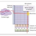
    Synopsys provides novel approach to accurately estimate delays of sub-circuits within a memory block and use the graph analysis techniques to identify the most and least critical paths and determine all timing violations in a fraction of time taken by any dynamic circuit simulator.

    The paths can extend from control logic through entire memory core to output buffers. The accuracy of result is again best within 5% of HSPICE. It supports both the approaches of memory model generation – characterization of memory compiler generated models and characterization of individual memory instances.

    In the STA flow for memory design and characterization, the tool uses Spice/FastSpice as a sub-ordinate tool to further analyze and fine tune the timing violations found in the design at the first place.

    Similarly memory compiler generated memory instances can also be characterized and verified by IP users.

    It supports both timing models – Composite Current Source (CCS) and the standard Non-linier Delay Models (NLDM). The CCS model proposed by Synopsys for nano-meter delay modelling can be found at – http://www.opensourceliberty.org/ccspaper/ccs_timing_wp.pdf

    The STA tool in NanoTime performs all types of timing checks pertaining to setup and hold times which are most crucial for the accuracy of sequential circuits. Several variants of these in the context of memory such as read / write time, read / write enable and so on; are all checked exhaustively and timing models are generated quickly for full-chip SoC sign-off. With all these kind of checks, it provides completeness on verification coverage as there are no vectors involved to be missed. It also checks Signal Integrity and does noise analysis. The tool has great capabilities in today’s context of designs.

    By Pawan Kumar Fangaria
    EDA/Semiconductor professional and Business consultant
    Email:Pawan_fangaria@yahoo.com


    EDPS Monterey. Agenda Now Available

    EDPS Monterey. Agenda Now Available
    by Paul McLellan on 03-12-2013 at 8:13 pm

    For 20 years there has been the Electronic Design Process Symposium. It has been held each April and for the last few years at least has always been in Monterey at the Monterey Beach Resort. This year it is Thursday and Friday April 18th/19th.

    The keynote on the first day is by Ivo Bolsens of Xilinx on The All-programmable SoC — at the Heart of Next-Generation Embedded Systems. The morning is then devoted to system and platform design, with presentations from Space Codesign and Cadence, and a panel session on How to make ESL really workwith Greg Wright of Alcatel, Mike McNamara of Adapt-IP, Gene Matter of Decoa Power, Guy Bois of Space Codesign, and Franck Schirrmeister of Cadence.

    After lunch it is all about Design Collaboration with presentations by Synopsys, Intel, Nimbic, Xuropan and NetApp.

    Then up into the 3rd dimension with a session on 3D system design, with presentations by Mentor, Cadence and Micron followed by a panel session 3DIC, are we there yet? with Dusan Petranovic of Mentor, Brandon Wang of Cadence, Mike Black of Micron, Ivo Bolsens the CTO of Xilinx, Gary Smith and Herb Reiter. Gene Jakubowski moderates.

    Gary Smith is giving the keynote during dinner on Silicon Platforms + Virtual Platforms = An Explosion in SoC Design.

    SemiWiki’s own Dan Nenni is giving the keynote on the second day on The FinFET value proposition. That is followed by a session on FinFET design challenges with presentations from Oracle, ARM, TSMC and Synopsys. Then after lunch the last session is on FinFET Foundry Design Enablement Challenges with presentations from 3 people from Global Foundries and ARM.

    The complete agenda is here. Early registration ends on March 18th so don’t wait too long before you decide to go. UPDATE: the EDPS website is in error, early registration ends on 31st. So jog don’t sprint.