Bronco Webinar 800x100 1

Samsung and the New World Order!

Samsung and the New World Order!
by Daniel Nenni on 03-12-2013 at 7:52 pm

The keynotes at CDNLive today were very interesting, but rather than cover the slides and bullet points let me share with you my personal view of Samsung and how they are changing the semiconductor industry. Before I continue remember I’m just a blogger who shares observations, experiences, and opinions. This blog is for entertainment purposes and not to be used for wealth management.

Right now Samsung Electronics is at $188B in revenue and expected to more than double in size by 2020. The Samsung Semiconductor portion is $33B and I predict that number will triple. To fuel that growth Samsung will spend hundreds of billions of dollars. Capital expenditures alone will be roughly $200B. That’s a lot of money folks and money talks!

If you look at Apple and how they completely remodeled the mobile industry, you will see the same pattern with Samsung and the electronics industry. Apple strategy focused on the “user experience” by controlling the associated ecosystem which brought us the iFamily of products: iPods, iPads, iPhones, iOS, iTunes, iCloud, etc… and hopefully iTV and the iWatch. All available online or in person at more than 400 Apple retail stores around the world. In owning the user experience Apple became what it is today, one of the most valued corporate brands.

Samsung is taking a similar route but not stopping at the ecosystem, they will control the entire electronics supply chain. If you were at the consumer electronics show this year you saw it up close and personal. The Samsung booth was ginormous with every electronic gadget and appliance you can imagine. Visit South Korea sometime and you will be hard pressed to see products in use that aren’t Samsung, even tooth brushes! If you look at the bill of materials for Samsung products you will see Samsung part numbers through and through, they control their supply chains, absolutely.

The fabless semiconductor industry started from IDMs renting out excess fab space and some say Samsung entered the foundry business for the same reason but I don’t agree. Samsung was founded in 1938 and is a very long term strategy company. Being an IDM certainly gives you depth in the semiconductor supply chain but even more so as a foundry. While other foundries built ecosystems organically over the years through partnerships and joint development activities, Samsung’s strength is inorganic business development (they can write some very big checks!)

Starting with EDA, “where electronics begins”, Samsung is one of the largest consumers of EDA tools and EDA really likes big checks. Samsung is now on the board of Cadence, right? Same goes for IP; ARM is the #1 CPU core for Samsung mobile products and look at all the ARM/Samsung 14nm press releases. ARM likes big checks too. Samsung also launched a $100M VC fund for semiconductor start-ups and you can bet they will include foundry services and EDA tool flows. Samsung knows how to invest so there are more big checks coming, believe it.

So where does that leave us folks in the fabless semiconductor ecosystem who traditionally do not write big checks? Or those of us who are not on the receiving end of those big checks? Well, may the force be with us!

Virtual Platforms, Acceleration, Emulation, FPGA Prototypes, Chips

Virtual Platforms, Acceleration, Emulation, FPGA Prototypes, Chips
by Paul McLellan on 03-12-2013 at 7:13 pm

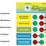
At CDNLive today Frank Schirrmeister presented a nice overview of Cadence’s verification capabilities. The problem with verification is that you can’t have everything you want. What you really want is very fast runtimes, very accurate fidelity to the hardware and everything available very early in the design cycle so you can get software developed, integration done and so on. But clearly you can’t verify RTL early in the design cycle before you’ve written it.


The actual chip back from the fab is completely accurate and fast. But it’s much too late to start verification and the only way to fix a hardware bug is to respin the chip. And it’s not such a great software debug environment with everything going through JTAG interfaces.

At the other end of the spectrum, a virtual prototype can be available early, is great for software debug, has reasonable speed. But there can be problems keeping it faithful to the hardware as the hardware is developed, and, of course, it doesn’t really help in the hardware verification flow at all.

RTL simulation is great for the hardware verification, although it can be on the slow side on large designs. But it is way too slow to help validate or debug embedded software.

Emulation is like RTL simulation only faster (and more expensive). Hardware fidelity is good and it is fast enough that it can be used for some software integration testing, developing device drivers etc. But obviously the RTL needs to be complete which means it comes very late in the design cycle.

Building FPGA prototypes is a major investment, especially if the design won’t fit in a single FPGA and so needs to be partitioned. So it can only be done when the RTL is complete (or close) meaning it is very late. In most ways it is as good as the actual chip and the debug capabilities are much better for both hardware and software.


So like “better, cheaper, faster; pick any two”, none of these are ideal in all circumstances. Instead, customers are using all sorts of hybrid flows linking two or more of these engines. For example, running the stable part of a design on an FPGA prototype and the part that is not finalized on a Palladium emulator. Or running transactional level models (TLM) on a workstation against RTL running in an FPGA prototype.

To make this all work, it needs to be possible to move a design from one environment to another as automatically as possible, same RTL, same VIP, even be able to pull data from a running simulation and use it to populate another environment. Frank admits it is not all there yet, but it is getting closer.

Now that designs are so large that even RTL simulation isn’t always feasible, these hybrid environments are going to become more common as a way to get the right mix of speed, accuracy, availability and effort.


Visually Debugging IC Designs for AMS and Mixed-Languages

Visually Debugging IC Designs for AMS and Mixed-Languages
by Daniel Payne on 03-12-2013 at 4:18 pm

With an HDL-based design methodology many IC engineers code in text languages like SystemVerilog and VHDL, so it’s only natural to use a text-based debug methodology. The expression that, “A picture is worth a thousand words” comes to my mind and in this case a visual debug approach is worth considering for AMS and mixed-language IC designs.

Let’s say that on your SoC project there are multiple IP blocks being re-used, and that they are coming from another design group, another design location, or even another company. How would you get up to speed in understanding not only the interconnects to the IP block, but also take a peek inside the IP to best understand the structure or behavior?

It would take way too long to directly read the text in SystemVerilog or VHDL, then create a graphical representation manually. You have better things to do with your engineering talent then manually visualize how an IP block was designed. The good news is that there is EDA technology available that can:

Read in a mixed-language netlist

  • SystemVerilog
  • VHDL

Read in a gate-level netlist

  • EDIF

Read in a transistor-level netlist

  • SPICE
  • HSPICE
  • Eldo

Read in interconnect netlist

  • DSPF

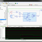
This EDA technology is called StarVision PROand is developed by a German-based company called Concept Engineering. I first met the President and CEO, Gerhardt Angst, several years ago when I worked at Mentor Graphics and we needed a way to visualize SPICE and DSPF netlists that were supplied by FastSPICE users.

We used SpiceVision PRO and it was the only automated method that we could find that would quickly and accurately create a SPICE netlist, on the fly, with very little learning curve. It was a real time-saver for us, because we could quickly visualize the unknown circuits being simulated at the transistor level, traverse the hierarchy, and understand more of the design intent of the netlist. The transistor-level netlists were easy to read, and the logic flowed naturally from left to right, as neatly as if someone had hand-drawn the schematics.


Gerhard Angst, Concept Engineering

Webinar
If you are debugging IP at the RTL, gate, transistor or interconnect levels, and want to save some time in that process, then plan to attend their webinar next week on Tuesday, March 12th, 10:00AM PDT. Registration is online, and will fill up fast, so attend and get your questions answered about how a visual debug approach will save you time and effort.


Cadence To Acquire Tensilica

Cadence To Acquire Tensilica
by Paul McLellan on 03-11-2013 at 5:54 pm

You have probably already seen the news: Cadence is acquiring Tensilica for $380M. Cadence has been relatively late to the IP party compared to Synopsys. In contrast, Mentor was early, got into the IP business before it was really profitable and ended up shutting down the business.

Tensilica is quite sizable. It has over 200 licensees, including 7 of the top 10 semiconductor companies. They announced earlier this year that they had shipped over 2 billion cores. Somebody asked me how this will affect Cadence’s relationship with ARM but I don’t really see them as equivalent. People use Tensilica’s dataplane processors for specialized functions such as audio, voice recognition, video and wireless modem, where the ARM processor is not especially well-suited. Synopsys’s ARC processor, acquired in the Virage deal, seems a closer match. Many chips use an ARM processor as a control processor and then have Tensilica cores for offloading, normally to reduce power or, sometimes, to get bring more processor horesepower to bear on a complex problem. And, in fact, the press release announcing the acquisition even has a quote from Simon Segars, the President of ARM, that this is positive for the industry.

It will be interesting to see whether Cadence’s large sales channel is able to get more design wins than Tensilica could as a small company. After all, it is not as if customers didn’t know Tensilica existed. I had the same questions about the Denali acquisition but everyone in Cadence seems to think that worked out well.

With Imagination acquiring MIPS, the processor world is getting a shakeup right now. it is going to be interesting to how this all plays out.

The press release on the acquisition is here. Also read A Brief History of Tensilica


Sanjiv Kaul: Is HLS About to Take Off?

Sanjiv Kaul: Is HLS About to Take Off?
by Paul McLellan on 03-10-2013 at 8:10 pm


At the end of last week I talked to Sanjiv Kaul, the new CEO of Calypto. Just to give a little background for those that haven’t been following along at home, Calypto was founded to try and solve the very hard problem of sequential logical equivalence checking (mostly by people from the engineering team that I managed at Ambit). SLEC is automatically comparing the C (or SystemC etc) input to high level synthesis (HLS) with the RTL output. They then took this technology and produced a sequential power reduction product, which was a much easier sell since it didn’t depend on the acceptance of HLS, it operated at the RTL level. Meanwhile, over at Mentor they developed an HLS product called Catapult that was having a hard time getting traction without a focused sales force. The Catapult product line and its people were transferred to Calypto in a complicated transaction so now Calypto has 3 product lines:

  • SLEC
  • PowerPro
  • Catapult


HLS has been bouncing along for years with early adopters and a slow adoption. The first product in the space, that was eventually canceled, was Synopsys Behavioral Compiler back in the mid-1990s. A decade ago everyone pretty much assumed that after RTL would come HLS and we’d move up a level. But in fact we switched to IP as a higher-level abstraction. But as IP blocks are now so large individually that we need to improve the productivity of creating them. When Sanjiv has been talking to customers, many are starting to be at that proliferation stage where their initial projects have been a success and now it is time to deploy widely across the company.

“RTL is the new netlist.” The process for getting from RTL to completed physical layout is now getting to be turnkey (of course the people turning the keys would argue it is really hard, and that is true, but it is not really where the value is added in the design). More and more of the differentiation is going on at the IP level and this is the big opportunity for HLS.

Since Catapult has the only SLEC product on the market, Sanjiv feels this means that they are the best positioned. Formal verification techniques tend to be hard to use without guidance from the synthesis tool, but until Catapult moved into Calypto it wasn’t possible to build in appropriate hooks. By more tightly integrating Calypto with both SLEC and with the sequential power reduction, a more powerful product can be made.

In the past, Sanjiv has taken multiple products to a market dominating position, such as PrimeTime or Physical Compiler at Synopsys. Of course he hopes that the magic will work again and feels Calypto is well positioned to be the standard HLS/SLEC tool, the winner in the space. But it is early and there are multiple players. It reminds him of the early days of logic synthesis when companies such as Silc, Trimeter, Mentor/Autologic were also around, before the market standardized on DC.

Calypto is profitable and cash-flow positive (which is actually more important in a startup). They are around 100 people.

There is a webinar coming up on March 26th at 10am Pacific on How to Optimize for Power with High Level Synthesis. More details here.


A Brief History of the Foundry Industry, part 2

A Brief History of the Foundry Industry, part 2
by Paul McLellan on 03-10-2013 at 8:05 pm

Part 1 here.

The line between fabless semiconductor companies and IDMs has blurred over the last decade. Back in the 1990s, most IDMs manufactured most of their own product, perhaps using a foundry for a small percentage of additional capacity when required. But their own manufacturing was competitive, both in terms of the capacity of fab they could afford to build, and in terms of process technology.

However, gradually both of these things changed. The size of fab required to remain cost-competitive continued to increase to the point that most semiconductor companies could not fill a fab that large. The semiconductor processes also got significantly more complex and costly, so that the cost of staying on the leading edge became prohibitive for all except the largest IDMs, most notably Intel.

The first thing that happened was the formation of several process clubs, where a lot of the cost of technology development of the semiconductor process could be shared between a number of semiconductor companies. A small semiconductor company couldn’t hope to develop a state-of-the-art process on their own.

Gradually it became clear that only the largest semiconductor companies could even afford to build a cost-competitive fab. It wasn’t just a matter of the investment required, it was that the capacity that they would create would be more than they would be able to use. They would never be able to “fill the fab.” Back when a fab cost $3B to build, that meant that roughly a company would face a depreciation cost of $1B per year, meaning that they need to have a running semiconductor business of perhaps $5B, around the size of AMD, the only competitor to Intel in the x86 microprocessor business.

In fact, in March 2009, AMD went completely fabless. They divested their manufacturing to the Advanced Technology Investment Company, primarily owned by the Emirate of Abu Dhabi. The manufacturing part became a pure-play foundry called Global Foundries. This was still partially owned by AMD and, of course, with AMD already had a large customer in place. Subsequently Global Foundries acquired Chartered Semiconductor, the other major pure-play foundry based in Singapore, and today they are the second largest foundry behind TSMC.

Many other semiconductor companies also went fabless, such as Freescale, Infineon and Sony. Other semiconductor companies didn’t go quite so far. They kept their existing fabs, many of which were fully depreciated and running non-leading-edge processes. But for the most advanced processes they used foundries since they couldn’t afford either the investment or the cost of technology development to keep up. These companies, still usually called IDMs, are known as fab-lite.

In 1994 the fabless semiconductor companies and the foundries created the Fabless Semiconductor Association. There was already an organization, the Semiconductor Industry Association, which most IDMs belonged to, but in that era, fabless semiconductor companies were not seen as “real” semiconductor companies and were not allowed to join. This has since been renamed the Global Semiconductor Alliance or GSA.

GSA’s data show that in 2012 the top foundry is TSMC by a long way, with revenues of $16B. Global Foundries is number two with revenues of $4.3B, followed by UMC with $3.7B. The fourth largest company in terms of foundry business is Samsung, which is an IDM. Their foundry business was $3.4B. Of course they are famously both a major supplier of chips to Apple and their primary competitor in the smartphone business. Number 5 is China-based SMIC, the only other company with foundry revenues over $1B, at $1.6B. The size of business drops off rapidly although there is a long tail of foundries. For example, in twelfth place is Korea-based MagnaChip with revenues of $375M, one fortieth the size of TSMC.

Meanwhile the transition of IDMs towards outsourcing manufacturing to foundries continues. At 45nm, nine semiconductor companies had their own 45nm fabs: Intel, Samsung, IBM, ST, Panasonic, Renasas, Texas Instruments, Toshiba and Fujitsu. By the 20/22nm process node, the only IDMs with their own fabs, ignoring specialist companies that only manufacture memories, are Intel, IBM and Samsung.

At 20/22nm, the foundry manufacturing has been taken up by TSMC, UMC, Global Foundries and Samsung, the only foundries with 20/22nm fabs in place or planned.

Meanwhile, more and more of the top ten of the non-memory semiconductor manufacturers are taken up with fabless and fab-lite companies. In 2011, the latest year for which data is available, Intel (IDM), Samsung (IDM and foundry) and Texas Instruments (fab-lite) take up the top three places. They are followed by Toshiba (fab-lite), Renasas (fab-lite), Qualcomm (fabless), ST (fab-lite) and Broadcom (fabless). Basically the rest of the top 25 are all either completely fabless or using the fab-lite approach of using foundries for leading edge process and continuing to manufacture internally anything that doesn’t require a leading-edge fab. IBM (IDM and foundry) slots in somewhere, but they consume so much of their silicon internally that it is not clear where. Their merchant business is not very large.

Going forward, it is unclear whether all the IDMs and foundries that have made the move to 20/22nm will also be able to afford to make the transition to 14nm and beyond. There are big technical challenges as well as economic issues as to what price wafers will cost and, as a result, just how much of the existing product lines will make the transition as opposed to remaining on cheaper, less advanced, process nodes.


We are Live at CDNLive 2013!

We are Live at CDNLive 2013!
by Daniel Nenni on 03-10-2013 at 7:00 pm

Dr. Paul McLellan and I will be covering CDNLive this week, one of the premier EDA events of the year. Take a look at the agenda and exhibits, this year it looks like a full on Design Automation Conference! There is definitely something for everyone!

Get ready for two full days of content with more than a hundred tracks and keynotes by Lip-Bu Tan, President and Chief Executive Officer, Cadence – Young Sohn, President & Chief Strategy Officer, Samsung Electronics – and Martin Lund Sr. Vice President, Research & Development, SoC Realization Group, Cadence.

What’s Happening at CDNLive Silicon Valley 2013:

March 12-13, 2013
Hyatt Regency
Santa Clara, CA

Papers: Choose from a wide variety of user-authored papers addressing all aspects of design and IP creation, integration, and verification. Discover how others are using Cadence technologies and techniques to realize silicon, SoCs, and systems—efficiently and profitably.

Techtorials: Participate in a variety of interactive techtorials to get a more in-depth look at specific Cadence products, new solutions, and feature enhancements.

Keynote speakers: Hear from industry leaders who influence the global electronics marketplace. They will discuss industry trends in silicon, SoC, and system realization and share their thoughts on the most pressing design challenges.

Designer Expo: Learn more about the collaborative ecosystem available to support you. Cadence and our partners will showcase the latest results of our joint efforts. Explore new products and services from our many exhibitors.

Networking opportunities: Engage in stimulating technology discussions with your peers and stay connected after the conference.

CONNECT. SHARE. INSPIRE.

Not only do Paul and I get in for free, we will be having lunch with Cadence executives (the privileges of blogging on SemiWiki). After lunch we get private briefings. Mine is with Martin Lund, if you have questions you would like asked let me know. Preferably ones that make me look smart!

Here are the tracks I’m most interested in:

MIX101 Data Management for Mixed-Signal Designs, ClioSoft, Inc.
SYS204 How ARM® Software Development Tools can Accelerate Your Time To Market ARM
AVD201 Technology and Design co-optimization for 10nm and Beyond GLOBALFOUNDRIES
AVD202 Designing with 14nm FinFET Technology Cadence
AVD203 14nm FinFET implementation of an ARM Cortex-A7 Samsung/Cadence
AVD204 Designing with Layout Dependent Effects (LDE) in TSMC Advanced CMOS Processes TSMC
SFF206 Scalable Power Sign-off Methodology for Ultra Large Design NVIDIA
AVD207 The DRC + Pattern Database GLOBALFOUNDRIES

CDNLive Silicon Valley brings together Cadence technology users, developers, and industry experts to network, share best practices on critical design and verification issues, and discover new techniques for realizing advanced silicon, SoCs, and systems. And, you’ll have the chance to talk directly with the Cadence technologists who develop your tools.

CDNLive Silicon Valley 2013 registration includes:

  • Attendance at keynote presentations
  • Access to Cadence R&D and technology experts
  • More than 80 technical sessions, techtorials, and demos
  • Access to the Designer Expo
  • Access to all networking event
  • Lunches and coffee breaks for the duration of the conference

If you have not registered for CDNLive yet you can do so HERE. Try the promo code DCPCDN13 for a reduced rate. See you there!


Reliability is the New Power

Reliability is the New Power
by Paul McLellan on 03-09-2013 at 9:56 am

It has be come a cliche to say that “power is the new timing”, the thing that keeps designers up at night and drives the major architectural decisions in big SoCs. Nobody is saying it yet but perhaps “reliability is the new power” will be tomorrow’s received wisdom.

I talked to Adrian Evans of IROCTech last week. He used to work at Cisco and with an enormous installed base of routers processing enormous amounts of data, very rare events such as Single Event Effects (SEE) happen all the time. And customers don’t like it when their routers reboot for no discernible reason, not to mention being very expensive for Cisco to swap out “faulty” boards that actually have no faults, just got hit by a random cosmic ray. The chips in those generations of routers are not even 28nm or 20nm, and SEE problems get worse with process generation, as the gate-oxide becomes just a few atoms thick, the power densities increase and lower voltages lead to lower noise margins. So one thing you will see is system companies such as Cisco specifying reliability standards for all chips.

Several years ago, when power really started to become the huge issue it is today, we developed power standards. Of course purchasers of chips would specify power numbers, especially for mobile devices, but the place that power really changed design was in building power delivery networks (and analyzing them), board design and a standard file format. Well, we are EDA, so we can never make do with one standard when two would be more fun, so we ended up with both CPF and UPF with broadly comparable capabilities as a way of specifying power policy throughout the design flow.

There is no equivalent format for specifying reliability data, constraints, policy etc throughout the design flow. You can go into PrimeTime and say “report_timing” or “report_power” but “report_reliability” won’t give you anything.


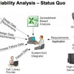
Like other things in design, reliability is a tradeoff. For chips in satellites, triple redundancy and voting might be appropriate to achieve extremely high levels of reliability in an extremely difficult environment, but it would be completely inappropriate for a cell-phone. In other environments, errors in the chip may not be so important if they can be detected and corrected in software. You can see that reliability is thus a chain from software down to chips down to things like making sure the solder in your package doesn’t emit too many alpha particles. As with any chain, it is only as strong as the weakest link. But the corollary is that there is no point in building one or two especially strong and expensive links, you want all the links to be roughly the same strength.

We are past the time at which spreadsheets and email work as a way of passing reliability data around. What is required is a Reliability Information Interchange Format (RIIF). Well, such a standard is, in fact, in development. It is a modeling language with a purpose to specify the rate of occurrence of failure modes in electronic components. The goal is to make it an eventual IEEE standard. Work started about a year ago, largely in conjunction with the European automotive manufacturers.


People expect their cars to last 10 or 20 years and much of the electronics in cars has to work in a fairly hostile environment, climbing out of death valley in summer means that the ECUs in the car are in a very hot environment, Minnesota in February not so much. And the electronics in cars (now well over 100 electronic control units or ECUs are in a high-end car) is, in many cases, safety critical. For sure, Cisco doesn’t want their routers to reboot unexpectedly. But you really don’t want your ABS system to reboot unexpectedly. So the automotive manufacturers are in the vanguard of driving reliability metrics down their supply chain.

There are two important workshops on this topic coming up this month, one in Silicon Valley and one in Europe in Grenoble:

  • Silicon Errors in Logic – System Effects (SELSE) at Stanford, March 26th and 27th. Details here. Keynotes from Microsoft, IBM and DoD CEC.
  • 1st RIIF Workshop, Grenoble, March 22nd (co-located with DATE). Towards Standards for Specifying and Modeling the Reliability of Complex Electronic Sytems. Details here. There are speakers from ARM, Intel, Bosch, Infineon Automotive among others.


Qualcomm and Intel Dynasty Scenario at 14nm

Qualcomm and Intel Dynasty Scenario at 14nm
by Ed McKernan on 03-08-2013 at 1:00 pm

At a different time, but certainly within the past 12 months, Paul Otellini was asked if Intel would be a Foundry for Qualcomm. His reply was that it did not leave a good taste in his mouth. Nevertheless it was not rejected and the door that remained open just a crack is likely to swing open for Qualcomm, the premier mobile silicon supplier in whom both Apple and Samsung are dependent, to win the Mobile Market. The hinge of fate rests in the hands of Andy Bryant, Chairman of Intel, who would need to EOL the Atom and the acquired Infineon baseband group to eliminate the competitive wall that would lead to not just a true Fab filling but would redraw the geopolitical map of the semiconductor industry. With Intel pouring another $13B of CapEx into its expanded 14nm footprint, there are only two possibilities that make sense: Qualcomm and Apple (the latter is now focused on TSMC). A marriage of Qualcomm baseband with Intel 14nm process technology could result in a scenario that would be a remake of Intel’s 1990s Pentium Dynasty.

The trend in the mobile industry for Samsung and Apple is to continue down the path of increased verticality. The Baseband Ecosystem maintains the high ground in tablets and smartphones and soon it will be a standard feature in x86 ultrabooks. Intel bought Infineon’s baseband group to complete the platform needed to compete in the broader mobile market. However, their efforts are still markedly behind that of Qualcomm and others. Bryant can continue the forced march with little to show or abandon the effort that blocks Qualcomm’s entry into the Fabs.

An article recently mentioned that Apple has hired a team of over 100 ex TI Engineers in Israel to create WiFi and Bluetooth solutions. The timeframe for these solutions is unknown but with $137B in the bank it is easy for Apple to acquire the talent that can create silicon solutions that end up replacing their current suppliers (i.e. Broadcom and Qualcomm). A net reduction of $20 of silicon in every iPhone, iPAD and perhaps Mac Airs could lead to saving the company up to $10B in the era of the Billion Unit+ mobile market that is arriving in the next couple of years. As they say a Billion here, a Billion there and pretty soon your talking real money.

The aggressiveness of Apple and Samsung in designing the key platform components while elbowing out other Fabless vendors at the Foundry has to be making Qualcomm nervous. The $25B+ in Qualcomm’s bank account leads all mobile players, except Apple. What if the cash is not enough of a cushion to prevent Apple or Samsung from hiring or buying the assets of Qualcomm’s competitors? If you think it unlikely, then one just has to review the staggering opportunity outlined above.

Under the Andy Bryant Regime, All product groups must now come clean on their true ROI of existing and new products. Atom processors fall way below the line of pulling their weight for a company that by next January will have spent $36B on Capex in the past three years. All of this to drive towards 22nm and 14nm dominance. In contrast to Atom, the Xeon and Ivy Bridge more than any other digital IC, except FPGAs, are delivering on a heavy positive cash flow. However, the dilemma in play is that mobile will be at least an order of magnitude larger than x86 powered PCs and the number of Fabs will matter in the end game.

The idea that a fast growing market could be on an accelerating path towards consolidation seems at odds with the concept that a rising tide lifts all boats. It took more than 50 years for the American auto industry to consolidate and yet the new mobile industry and the entire supply base may do so in less than 8 years from the time of the first iPhone introduction. It is in Apple and Samsung’s interest to accelerate the trend.

Juxtaposed to the Samsung and Apple vertical supply chain is the also heavily capitalized Fabs of Samsung, TSMC and Intel who race to be the ultimate winner at the leading edge, where all mobile silicon goes to maximize performance/watt while minimizing quiescent current. Intel’s leadership in the pre-mobile days was based on the x86 processor lock required for Windows and its process lead. The silicon supremacy shift away from processors and to the baseband and wireless infrastructure occurred faster than most imagined and the Intel acquisition of Infineon has proved to be too late in the game to help x86 Atoms make a dent in the market.

Now that the multi-billion unit, 4G enabled train has left the station, Intel has to catch up with its only true weapon and that is 14nm. Should Andy Bryant be able to sign a Foundry agreement with Qualcomm and redirect Intel’s massive design resources, there would be benefits in a number of areas for both companies. For Qualcomm, the ability to leverage Intel’s lower cost and much lower power 14nm would remove the competitive threats of Broadcom, nVidia, Mediatek and others. Samsung and Apple would have to think twice of continuing with their own internal wireless and baseband developments as Qualcomm moves into the mid range and low end markets at generous margins. The profit pool that would arise for Intel and Qualcomm would be staggering but it requires Intel give up its desire to own the chip inside the smartphone.

In return for enabling Qualcomm to clear the field, Intel would take a giant step towards rebalancing its Fabs relative to Samsung and TSMC in the mobile market. This move, with Qualcomm’s increased TAM exposure at the expense of its rivals, would be the equivalent of moving more than one Fab loading from TSMC over to Intel’s side of the ledger. For Intel the legacy x86 and Data Center business will still require some leading edge capacity, however a larger and larger percentage of processors will shift to a longer tail business model now that AMD competition has melted away. Intel will initiate other long tail fab deals, of which the 14nm Altera one is a perfect example.

The outcries from the former Otellini regime will be huge as the Atom and Infineon groups fight to remain relevant. The math is simple for Bryant. A $15 Atom processor at 5-10% or even 20% share in the smartphone market doesn’t come close to the revenue and margins that are available by opening up the Foundry to Qualcomm. Legacy Intel and Windows will remain together from tablets to PCs and servers as Win RT on ARM fades quickly into the sunset. By the end of 2013, I can envision a scenario where the partnership of Intel and Qualcomm is announced and the surprise to most is that they are no longer competitors at the platform level.

The tremors that will ripple through the semiconductor industry on an Intel – Qualcomm partnership will destabilize much of the mobile market and over time be seen as greater in magnitude than any other single event, including IBM’s selection of Intel’s 8088 for the original PC that sent Motorola packing. Qualcomm building products at Intel will lay low their wireless peers while Samsung and Apple take time to reconsider if their internal efforts are effectively moot. Intel’s ability to finally monetize its leading edge process will force Wall St. analysts to reconsider their valuation metrics. Beyond this though are additional second order derivatives acting as forcing functions. Will Apple consider a partnership at Intel so that they can develop the equivalent of a Snapdragon with their own ARM processor integrated with Qualcomm’s baseband?

For those of us who have watched the Semiconductor paint dry during the post Y2K decade, it is very interesting to consider what changes may occur as 14nm rolls out.

Full Disclosure: I am Long AAPL, QCOM, ALTR, INTC


Silicon Summit April 18th, 2013

Silicon Summit April 18th, 2013
by Daniel Nenni on 03-07-2013 at 7:00 pm

Moore’s Law has transcended computing expectations; however, its promise will eventually reach scalability limitations due to extraordinary consumer demands. Future technology encompasses breakthroughs capable of interaction with the outside world, which the More than Moore movement achieves. Through integrating functionalities that do not scale to deliver cost-optimized and value-added system solutions, this trend holds significant potential for the industry. This event will explore the business and technical factors defining the More than Moore movement, and address how it will yield revolutionary electronic devices.

Collaboration is the foundation of the fabless semiconductor ecosystem. TheGlobal Semiconductor Alliance continues to lead the way with Silicon Summits, technology work groups, and a comprehensive set of resources for the greater good of the industry that brought us the mobile devices that my children cannot live without!

GSA’s WORKING GROUPS

GSA’s Resources include:

The next Silicon Summit is April 18th, 2013 at the Computer History Museum. Reserve your seat now! GSA members receive complimentary admission. Non-member registration fee is $50. More than two hundred of the top semiconductor professionals will attend making this one of the best semiconductor ecosystem networking events.

Session One:Disruptive Innovation – Enabling Technology for the Mobile Industry of Tomorrow
With the industry’s long-term focus on scaling now joined by functional diversification, this session will open with an overview on how More than Moore is enabling the mobile landscape of today and shaping the future of tomorrow.

A panel will follow, discussing current and emerging applications that continue to drive the More than Moore adoption as well as the process technologies enabling this development.

Session Two: How More than Moore Impacts the Internet of Things
From the Swarm Lab to the smart bulb, the Internet of Things is showing evidence of becoming a reality. However today’s productivity trails what is needed to make the Internet of Things a truly ubiquitous system, and at the heart of the matter is developing the low power, mixed-signal technology that will enable chips and systems to communicate to the real world with minimal or without battery power. This session will open with an overview on where the industry stands in applying the concept of More than Moore to drive the Internet of Things.

A panel will follow, assessing the industry requirements, obstacles, and advancements in developing the technology required to make the Internet of Things a reality.

Session Three: Integration Challengesand Opportunities
Furthering the advancement of More than Moore involves unifying silicon technologies with novel integration concepts; application software convergence; and new supply chain business models. This session will open with an overview identifying the key industry trends, challenges and opportunities to realize higher density, greater functional performance and boosted power for ICs.

A panel will follow, discussing possible collaborative solutions to the challenges of integration and its impact on business market growth and investment.

Program:
View speaker bios.
[TABLE] style=”width: 100.0%”
|-
| Time
| Item
| style=”width: 23px” |
|-
| 9:00 a.m.
| Registration
|
|-
| 9:15 a.m.
| colspan=”2″ | [TABLE] style=”width: 100.0%”
|-
| Morning Reception sponsored by SuVolta
|
|-

|-
| 9:45 a.m.
| Opening Remarks
|
|-
| 10:00 a.m.
| Session One: Disruptive Innovation – Enabling Technology for the Mobile Industry of Tomorrow
|
|-
|
|

  • Kaivan Karimi, Executive Director, Global Strategy & Business Development, Microcontroller Group, Freescale

|
|-
|
|

|
|-
|
|

|
|-
|
|

  • Dr. Ely Tsern, VP & Chief Technologist, Memory and Interfaces Division, Rambus

|
|-
| 11:00 a.m.
| Networking Break
|
|-
| 11:15 a.m.
| Session Two: How More than Moore Impacts the Internet of Things

Moderator:Edward Sperling, Editor In Chief, Low-Power Engineering
|
|-
|
| Panelists:
|
|-
|
|

|
|-
|
|

  • Kamran Izadi, Director, Sourcing & Supplier Management, Cisco

|
|-
|
|

  • Oleg Logvinov, Director of Market Development, Industrial and Power Conversion Division, STMicroelectronics

|
|-
|
|

  • Martin Lund, Senior VP, Research and Development, SoC Realization Group, Cadence

|
|-
| 12:15 p.m.
| Networking Lunch
|
|-
| 1:15 p.m.
| Session Three: Integration Challenges and Opportunities

Moderator:Bruce Kleinman, VP, Product Marketing, GlobalFoundries
|
|-
|
| Panelists:
|
|-
|
|

|
|-
|
|

|
|-
|
|

|
|-
|
|

|
|-
| 2:15 p.m.
| Closing Remarks
|
|-

The Global Semiconductor Alliance (GSA) mission is to accelerate the growth and increase the return on invested capital of the global semiconductor industry by fostering a more effective ecosystem through collaboration, integration and innovation. It addresses the challenges within the supply chain including IP, EDA/design, wafer manufacturing, test and packaging to enable industry-wide solutions. Providing a platform for meaningful global collaboration, the Alliance identifies and articulates market opportunities, encourages and supports entrepreneurship, and provides members with comprehensive and unique market intelligence. Members include companies throughout the supply chain representing 25 countries across the globe. www.gsaglobal.org