Bronco Webinar 800x100 1

Tanner EDA v16 OpenAccess is here!

Tanner EDA v16 OpenAccess is here!
by Daniel Nenni on 03-07-2013 at 4:00 pm

Tanner EDA is a pleasure to work with, they are big on collaboration and customers absolutely love their tools. With the Synopsys acquisition of SpringSoft, Tanner needs to step up and fill the void of the affordable Laker tools. Take a close look at their new v16 release and let me know how they are doing.

New capabilities for back-end (layout):

  • OpenAccess database support for PDK and EDA tool interoperability
  • Collaborative design / multi-user design control for enhanced team productivity
  • Improved file loading and rendering speeds
  • Improved performance of physical verification (HiPer Verify)

New capabilities for front-end (schematic capture, simulation, waveform viewing):

  • Integrated mixed-signal simulation (Verilog-AMS co-simulation)
  • Parametric plots, scatter plots and improved text control and graphics manipulation

Bottom line: OA for L-Edit provides a quantum leap in interoperability and productivity for designers and layout engineers. Design elements (and entire designs, in fact) can be dynamically created, modified and shared across and outside of a design team. Users of other layout tools can access and exchange the information seamlessly; provided those tools also support the Si2 OpenAccess database standard.

The feedback from first release customers is looking good:

HiPer Silicon v16 with OpenAccess provides users with unprecedented interoperability and advanced capability, offering an alternative tool flow for those seeking high productivity with improved price-performance. Whether designing IP blocks, discrete circuits or complete SoCs, OpenAccess designs can be easily shared between designers and engineering teams across other tool flows. As Kenton Veeder of Senseeker Engineering, Inc. said, “I really like the OpenAccess capabilities. I also like the increased control over axis labels in [waveform editor]W-Edit.” Veteran user Mark Wadsworth, Tangent Technologies founder, commented, “Overall v16 is a winner – great job Tanner EDA!”

There is a full suite of videos on the new features:

Mixed Signal Simulation Demo
L-Edit Standard & Custom Vias
L-Edit Library & Cell List Navigation
L-Edit Electrical Ports & Text Labels
L-Edit Open Access Databases
L-Edit Dockable Toolbars
S-Edit Verilog AMS views
W-Edit Plot & Curve Enhancements
W-Edit Parametric & Scatter Plots
W-Edit Measure Fit Calculation
W-Edit Cursor Table
W-Edit Chart Text Enhancements

Or you can register and see the Tanner Tools v16 Full Flow Demonstration. Better yet, take the Tanner tools for a free 30 day test drive!

Tanner EDA provides a complete line of software solutions that catalyze innovation for the design, layout and verification of analog and mixed-signal (A/MS) integrated circuits (ICs). Customers are creating breakthrough applications in areas such as power management, displays and imaging, automotive, consumer electronics, life sciences, and RF devices.

A low learning curve, high interoperability, and a powerful user interface improve design team productivity and enable a low total cost of ownership (TCO). Capability and performance are matched by low support requirements and high support capability as well as an ecosystem of partners that bring advanced capabilities to A/MS designs.


Multiprotocol 10G-KR and PCIe Gen-3 PHY IP will support big data and smartphone explosion

Multiprotocol 10G-KR and PCIe Gen-3 PHY IP will support big data and smartphone explosion
by Eric Esteve on 03-07-2013 at 7:47 am

We have frequently said in Semiwiki how crucial is it for the SC industry to benefit from high quality PHY IP… even if, from a pure business point of view (MBA minded), PHY IP business does not look so attractive. In fact, to be able to design on-the-edge SerDes and PLL (the two key pieces), you need to build and maintain a highly skilled and well experienced design team, benefiting of salaries in the top range of the industry, the EDA toolset needed to support high end analog design is also in the high range. On top of these needs to support the design phase, you also need to build a characterization lab, filled with expensive oscilloscopes able to track ps jitter and calculate BER…

Finally, because analog world is like the real world, that is, more unpredictable than the digital, the risk of redesign is far to be null! But, if you want to be able to support the ever increasing need for data bandwidth linked with the smartphone usage explosion and the requirement for accessing data in the cloud, you simply need to benefit from higher speed protocols, like 10G-Base KR or PCIe Gen-3, and to be able to create efficient systems, you need to integrate PHY supporting up to 10 Gbps data rate. A country based industry not able to design such high speed PHY IP would be like some other industries being forced to import from other countries the rare earth material absolutely essential to build key aeronautic, defense or communication systems …

Looking at a single channel PHY block diagram makes you disappointed? You think that a PHY design does not look that complex? In fact, some of the most important features are difficult to highlight in a block diagram, like:

  • Multi-featured (CTLE and DFE) receiver and transmitter equalization: adaptive equalizers have many different settings, and in order to select the right one there needs to be some measure of how well a particular equalization setting works. The result will be to improve Rx jitter tolerance, ease board layout design, and improve immunity to interferences.
  • Mapping the signal eye and output the signal statistics via the shown JTAG interface: this allows for simple inspection of the actual signal. This in-situ testing method can replace very expensive test equipment (when a simple idea gives the best results!)
  • The pseudo-random bit sequencer (PRBS) generator send patterns to verify the transmit serializer, output driver, and receiver circuitry through internal and external loopbacks (keep in mind that Wafer level Test equipment are limited in frequency range, such a circuitry allows running test at functional speed on a standard testers).

If you are interested by Eye diagram measurement, and more specifically want to know how to reduce PCI Express 3 “fuzz” with multi-tap filters, you definitely should read this blog from Navraj Nandra (Marketing Director PHY & Analog IP with Synopsys). The very didactical article explains how adaptative equalization works, Inter Symbol Interferences (ISI), as well as help to understand how signals contain different frequency content, illustrated by four examples of forty bit data patterns, from the Nyquist data (data pattern alternating 1010 data) which is the data pattern which has the highest frequency content possible to the pattern integrating 20 ’0′s followed by 20 ’1′s, which represents the signal with the lowest frequency content. Navraj has been able to explain advanced signal processing concepts by using simple words, and this is everything but simple to do!

If you just want to know what are the protocols supported by the multi-rate PHY IP spanning 1.25 Gbps to 10.3 Gbps data rates to cover key standards: PCI Express 3.0, 10GBASE-KR, 10GBASE-KX4, 1000BASE-KX, CEI-6G-SR, SGMII and QSGMII, just download the “Enterprise 10G PHY IP” datasheet here, or have a look at this PR from Synopsys…

Eric Esteve from IPNEST


A Brief History of the Foundry Industry, part 1

A Brief History of the Foundry Industry, part 1
by Paul McLellan on 03-06-2013 at 2:10 pm

The fundamental economics of the semiconductor industry are summed up in the phrase “fill the fab.” Building a fab is a major investment. With a lifetime of just a few years, the costs of owning a fab are dominated by depreciation of the fixed capital assets (the building, the air and water purification equipment, the manufacturing equipment etc). This puts a big premium on filling the fab and running it as close to capacity as possible. If a fab is not full then the fixed costs will overwhelm the profit on the capacity that is used and the fab will lose money. Of course, if demand is high there is a corresponding problem since a fab that is already full cannot manufacture any more by definition (actually fabs sometimes run at 110% capacity but that is about the most that can be pushed through).

The capacity of a fab is usually a good fraction of the overall needs of the company that built it and so there is often a mismatch between the capacity needed, in terms of wafer-starts, and what is available. In one case, the semiconductor company is out of capacity, the fab is full, but they could sell more product if only they could get it manufactured. In the other case, the company has surplus capacity, perhaps a newly opened fab, and doesn’t have enough product to keep the fab full. This dynamic led to the original foundry businesses, which was semiconductor companies, sometimes competitors, buying raw manufactured wafers off each other to smooth out these mismatches between capacity and demand.

The first fabless semiconductor companies such as Chips & Technologies and Xilinx extended this model a little bit. By definition they didn’t have their own fabs, but they would form strategic relationships with semiconductor companies that had excess capacity. The relationships had to be strategic by definition. You couldn’t just walk into a semiconductor company and ask for a price for a few thousand wafers, any more than today you can walk into, say, Ford and ask how much to have a few thousand cars manufactured. It is not how they are set up to do business.

In 1987 a major change took place with the creation of the Taiwan Semiconductor Manufacturing Company, TSMC. It was an outgrowth of Taiwan’s Industrial Technology Research Institute, ITRI. Since very few fabless semiconductor companies existed back then (Chips and Technologies was founded only in 1985 for instance) their business model was to be a supplier to the existing foundry business, namely providing manufacturing services to semiconductor companies who were short of capacity in their own fabs. One of the original investors was Philips Semiconductors (since spun-out from Philips as NXP) who also was one of the first customers buying wafers.


United Microelectronics Corporation, UMC, was an earlier spinoff from ITRI, created in 1980 as Taiwan’s first semiconductor company. Across the road in Hsinchu from TSMC, its focus also gradually shifted to foundry manufacturing especially once the fabless ecosystem created both a lot of demand and also a wish to have a competitor to TSMC to ensure that pricing remained competitive.

The third of the big three back in that era was Chartered Semiconductor, based in Singapore and backed by a consortium including the Singapore government who saw semiconductor manufacture as a strategic move up the electronic value chain.

The big change that the creation of TSMC made was that it became possible to have semiconductor wafers manufactured without requiring a deep strategic relationship. Pricing wasn’t so transparent that you could just look at the price-list on the web (not least because in 1987 there wasn’t a web) but a salesman would quote you for whatever you needed. It was very similar to a metal foundry, where the name had come from: if you wanted some metal parts forged then they would give you a quote and build them for you. In the same way, if you needed some wafers manufacturing you could simply go and get a price.

This might not seem like that significant a change but it meant that forming a fabless semiconductor company no longer depended on the founders of the company having some sort of inside track with a semiconductor company with a fab, they could focus on doing their design safe in the knowledge that when they reached the manufacturing stage that they could simply buy wafers from TSMC, UMC or other companies that had entered the foundry business.

Companies such as TSMC and UMC were known as pure-play foundries because they didn’t have any other significant lines of business. Semiconductor companies with surplus capacity would still sell wafers and run their own foundry businesses but they were always regarded as a little bit unreliable. Everyone suspected that if the semiconductor company’s business exploded that they would be forced out and have to find a new supplier. Gradually, over time, the semiconductor companies whose primary business was making their own chips became known as Integrated Device Manufacturers or IDMs. This contrasted them with the fabless ecosystem where the companies that created and sold the designs, the fabless semiconductor companies, were different from the companies that manufactured them, the foundries.

The line between fabless semiconductor companies and IDMs has blurred over the last decade. Back in the 1990s, most IDMs manufactured most of their own product, perhaps using a foundry for a small percentage of additional capacity when required. But their own manufacturing was competitive, both in terms of the capacity of fab they could afford to build, and in terms of process technology.

Part 2 is HERE.

Also read: Brief History of Semiconductors


Lithography from Contact Printing to EUV, DSA and Beyond

Lithography from Contact Printing to EUV, DSA and Beyond
by Paul McLellan on 03-05-2013 at 6:21 pm

I used my secret powers (being a blogger will get you a press pass) to go to the first day of the SPIE conference on advanced lithography a couple of weeks ago. Everything that happens to with process nodes seems to be driven by lithography, and everything that happens in EDA is driven by semiconductor process. It is the place to find out if people believe EUV is going to be real (lots of doubt), how about e-beam, is directed self-assembly really a thing.

The keynote was by William Siegle called Contact printing to EUV and was a history and lessons learned from a career from when lithography started to the present day (well, a little bit into the future even).

Back when ICs first started, the technology was 1X contact printing. The mask would physically be in contact with the wafer (like a contact print in photography before everything went digital). The design was actually hand-cut out of a red plastic called rubylith (originally a trademark like escalator) at 5X the actual size. This would then be photographically reduced to create the master mask. The master mask would then be used to create submaster masks. And the submaster masks used to make working masks. The working masks didn’t last very long because they were physically in contact with the wafer and so would get damaged and pick up defects fast. One lesson was to beware 1X printing.

IBM decided that the thing to do was to use the technology used to make the mask, photoreduction, to build a stepper (although I don’t know if they used that name back then). But it turned out to be much harder than they thought and the project failed. Perkin-Elmer were the first to build a successful optical projection stepper. It was still a 1X reduction, the polygons on the mask the same size as on the wafer, but the mask didn’t contact the wafer so the damage/defect problem was much reduced.

Late 1970s steppers finally make it into production. Embarrassingly for the US, Nikon and Cannon soon had better machines than GCA and PE and dominated the market by the late 1980s. In the mid-1980s ASML emerged (and absorbed PE).

The US got seriously worried about the Japanese, not just in steppers but in semiconductor memory too. Until that point there had been no co-operation among companies but that was about to change. SRC, Sematech, DOD VHSIC program, IMEC, LETI, College of nanoscale science and engineering (CNSE) at University of Albany. Another lesson was that sharing enables faster progress.

There was dramatic advances in the 1990s as we went from 365nm to 248nm to 193nm light (we are still at 193 today) along with continual improvement in the photoresist, most notably the invention of CAR (chemically amplified resist) and excimer lasers. IBM actually had all this but kept it secret until they realized that the equipment industry would never build the equipment they needed at IBM until good resist was widely available.

There were some blind alleys too. Ebeam was used in the mask shop and everyone wondered if it would make it to the production flow. The challenge with e-beam is resolution versus throughput. If the beam is small, the throughput is low. As we moved to smaller nodes, e-beam became non-competitive.

The big blind alley was X-ray lithography (around 1nm wavelength). This was killed by three things. Firstly, it needed a synchrotron as a source of X-rays. Second, it required a 1X membrane mask. And remember, beware of 1X printing. But mostly it was built on a false assumption that we would not be able to get beyond 0.25um using optical technology. Well, we are pretty much at 14nm using that technology which is 0.014um in old currency. So one more lesson was to never underestimate the extendability of existing technology.

What has enabled light to last so long was a combination of optimizing the mask (optical proximity correction, OPC) and holistic litho optimization.

There are also promising future technologies. Nano-imprint has remarkable image fidelity (where the mask essentially is pressed onto the wafer). But it has all the same problems as the rubylith era, of 1X contact printing meaning that masters, submasters and working masks are required.

Of course the big hope for the future is EUV with a wavelength of 13.5nm with a 4X reduction reflective reticle. But we need to get the light source power up to 100-250W, we need production worthy masks, resists and metrology. The justification is economic, to avoid multiple patterning, but that it won’t be adopted until it can beat that cost ceiling.

And the future? Another rule, it is impossible to predict 10 years ahead. So at this point we can’t tell if EUV will make it, if directed self-assembly will turn out to be a breakthrough, if carbon nanotubes can be manufactured into circuits economically. We can really only see out about 3 years.


Verification the Mentor Way

Verification the Mentor Way
by Paul McLellan on 03-05-2013 at 3:05 pm

During DVCon I met with Steve Bailey to get an update on Mentor’s verification. They were also announcing some new capabilities. I also attended Wally Rhines keynote (primarily about verification of course, since this was DVCon; I blogged about that here) and the Mentor lunch (it was pretty much Mentor all day for me) on the verification survey that they had recently completed.

Verification has changed a lot over the past few years. The techniques that were only used by the most advanced groups doing the most advanced designs have become mainstream. Of course this has been driven out of necessity, as verification has expanded to take up more and more of the schedule. This is evident in the 75% increase in the number of verification engineers on a project since 2007, compared to the minor increase in the number of design engineers.


The specification for many designs is that each block must have 100% coverage, or waivers are required. Generating and justifying waivers to “prove” that certain code is unreachable and so does not need to be covered is very time consuming. NVidia estimated that they took 9 man-years on code-coverage on a recent project. So one new development is Questa CoverCheck that automates coverage closure. Formally generated waivers for unreachable code reduce the effort to write manual tests and also eliminates the tedious manual analysis to justify waivers to management.


Another new capability is in the area of interconnect verification. Trying to set up all the blocks on a modern SoC so that they generate the required traffic on the interconnect is very time-consuming to do by hand. The simulation is also large, requires a lot of memory and runs slowly. Instead, inFact can be used to generate the traffic more explicitly, replacing the actual blocks of the design with traffic generators that work much more directly.


Mentor also has tools for rules-based verification that gives verification engineers and, especially, the project management insight into how far along verification really is. When this is done ad hoc it always seems that verification is nearly complete for most of the schedule. As the old joke goes, it takes 90% of the time to do the first 90% of the design, and then the second 90% of the time to do the remaining 10%. By switching to rules-based verification the visibility is both improved and made more accurate.


Watch the Clock

Watch the Clock
by Paul McLellan on 03-05-2013 at 2:24 pm

Clock gating is one of the most basic weapons in the armoury for reducing dynamic power on a design. All modern synthesis tools can insert clock gating cells to shut down clocking to registers when the contents of the register are not changing. The archetypal case is a register which sometimes loads a new value (when an enable signal is present, for example) and otherwise recirculates the old value back from the output. This can be replaced with a clock gating cell using the same enable so that the register is only clocked when a new value is loaded, and instead of recirculating the old value the register is simply not clocked at all so that it retains the old value.

The efficiency of clock gating can be measured by clock-gating efficiency (CGE). Static CGE simply counts up the percentage of registers that are gated. But not every clock gate has much effect. In the archetypal example mentioned earlier, there is little power saving if the register loads a new value almost all the time, and a huge saving if the new value is almost never clocked in. Instead of using static CGE, dynamic CGE, the percentage of time that the clocks are actually shut off, is a much better measure.

But even dynamic CGE ignores just how much power is actually saved. If the enable signal shuts off a large part of the clock tree then the power saving can be large and it is worth the effort to try and improve the enable signal so that it captures all the times that the clock can be suppressed. On the other hand, if an enable only applies to a small part of the design (perhaps just a single flop) then there is little point in trying to optimize the enable (and, in fact, just clock gating the register may not even save power versus leaving the multiplexor to recirculate the output bit).

To perform this analysis most accurately requires clock-tree synthesis (CTS) to have been completed. But this is part of the physical design flow and is too late to return to the RTL level to optimize the RTL to incrementally reduce power. Instead, Apache’s PowerArtist allows this analysis to be done at the RTL level using models of the clock tree and the associated interconnect capacitance. This allows the enable efficiency to be calculated for each clock gate and highlights the cases where a gate controls a large amount of capacitance and so is a candidate for additional effort to further improve the enable efficiency and so further reduce power.

See Will Ruby’s blog on clock gating here.


Integrating Formal Verification into Synthesis

Integrating Formal Verification into Synthesis
by Paul McLellan on 03-05-2013 at 1:29 pm

Formal verification can be used for many things, but one is to ensure that synthesis performs correctly and that the behavior of the output netlist is the same as the behavior of the input RTL. But designs are getting very large and formal verification is a complex tool to use, especially if the design is too large for the formal tool to take in a single run. This is an especially severe problem for Oasys RealTime Designer because its capacity is so much larger than other synthesis tools. Using formal verification typically requires complex scripting and manual intervention to get results with reasonable runtimes.

Oasys and OneSpin Solutions have just announced an OEM agreement. Now, in EDA, OEM agreements really only work when the product being sold is integrated inside another (such as Concept Engineering’s schematic generator). Otherwise customers always prefer to buy the two products from their respective companies. This OEM is a tight integration. OneSpin is licensing a portion of its OneSpin 360 EC technology, automated functional equivalence checking software, to Oasys to integrate with RealTime Designer.


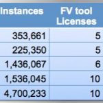
The integrated product allows RealTime Designer to drive the formal verification process automatically, dividing the design up into portions that can then be verified in parallel using multiple licenses. For example, a nearly 5 million instance design (so perhaps 30 or 40 million gates) can be verified in just over 2 hours using 10 licenses. The integration is fully compatible with the low power and DFT flows in RealTime Designer, correctly handling clock gating and scan chain insertion.

OneSpin EC equivalence checking ensures that the RTL design and the output gate-level netlist will produce the same results for the same inputs under all circumstances. It doesn’t use simulation-type approaches but is based on mathematically proving that this is so. In the event that this isn’t so (which would be a bug in RealTime Designer unless any manual intervention has taken place) it will produce a counter example.


Image Sensor Design for IR at Senseeker

Image Sensor Design for IR at Senseeker
by Daniel Payne on 03-05-2013 at 10:30 am

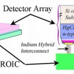
Image sensors are all around us with the cell phone being a popular example, and 35mm DSLR camera being another one. Last week I spoke with Kenton Veeder, an engineer at Senseeker that started his own image sensor IP and consulting services company. Instead of focusing on the consumer market, Kenton’s company does sensor design work for the military and scientific markets.


Read Out Integrated Circuit (ROIC) Continue reading “Image Sensor Design for IR at Senseeker”


Cavium Adopts JasperGold Architectural Modeling

Cavium Adopts JasperGold Architectural Modeling
by Paul McLellan on 03-05-2013 at 7:00 am

Cavium designs some very complex SoCs containing multiple ARM or MIPS cores at 32 and 64 bit. This complexity leads to major challenges in validating the overall chip architecture to ensure that their designs will meet the requirements of their customers once they are completed, with performance as high as 100Gbps.

Cavium have decided to use Japer’s JasperGold Architectural Modeling App to allow their architects to better specify, model and verify the complex behavior of these bleeding edge designs. I’ve written before on how ARM has been using Jasper’s architectural modeling to verify their own cache protocols (and, indeed, found some corner-case errors that all their other verification had missed). Cavium’s multi-core, multi-processor chips for sure have very complex interconnection protocols between the processors and memories.


The JasperGold Architectural Modeling App provides an easy and well-defined methodology for an efficient modeling and verification of complex protocols. Jasper’s Modeling App models a large part of the protocol much faster and with less effort compared to other modeling and validation methods. It captures protocol specification knowledge at the architectural level; performs exhaustive verification of complex protocols against the specification; creates a golden reference model that can be used in verifying the RTL implementation of the protocol; and automates protocol-related property generation and debugging aids.


Synopsys ♥ FinFETs

Synopsys ♥ FinFETs
by Daniel Nenni on 03-03-2013 at 6:00 pm

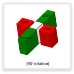
FinFETs are fun! They certainly have kept me busy writing over the past year about the possibilities and probabilities of a disruptive technology that will dramatically change the semiconductor ecosystem. Now that 14nm silicon is making the rounds I will be able to start writing about the realities of FinFETs which is very exciting!


From Moore’s Law, we can infer that FinFETs represent the most radical shift in semiconductor technology in over 40 years. When Gordon Moore came up with his “law” back in 1965, he had in mind a design of about 50 components. Today’s chips consist of billions of transistors and design teams strive for “better, sooner, cheaper” products with every new process node. However, as feature sizes have become finer, the perils of high leakage current due to short-channel effects and varying dopant levels have threatened to derail the industry’s progress to smaller geometries.

Synopsys published an article FinFET: The Promises and the Challenges which is a very good primer and talks about the FinFET Promise:

Leading foundries estimate the additional processing cost of 3D devices to be 2% to 5% higher than that of the corresponding Planar wafer fabrication. FinFETs are estimated to be up to 37% faster while using less than half the dynamic power or cut static leakage current by as much as 90%.

The foundries, on purpose or by accident, made the right decision in taking the 20nm planar process and adding FinFETs. Ramping a new process and a new 3D transistor would have been daunting for the SoC based fabless semiconductor ecosystem. Even for Intel, they may have 22nm Tri-Gate microprocessors but I have yet to see a 3D SoC from them. FinFET Design enablement (EDA and IP) is a big part of that transition and I have to give Synopsys the advantage here.

The foundry’s intent is to ensure the transition to FinFET is as transparent as possible, allowing users to seamlessly scale designs to increasingly smaller geometry processes. Maximum benefits with this technology will require implementation tools to minimize power consumption and maximize utilization and clock speed. FinFETs require some specific enhancements made in the following areas: TCAD Tools, Mask Synthesis, Transistor Models, SPICE Simulation Tools, RC Extraction Tools and Physical Verification Tools.


Synopsys building critical IP mass over the years, especially buying Virage Logic, has given them an early and intimate look at the bleeding edge of process development. Yes I have seen fluffy 14nm test chip press releases from all vendors but the foundation IP (SRAM) is where the rubber first meets the road and that gives Synopsys a lead on tool development.

That is why I asked Raymond Leung, VP of SRAM development at Synopsys, to present at the EDPS Conference FinFET Day that I’m keynoting. Not only does Raymond have deep SRAM experience from Virage, he also led SRAM development at UMC. At Synopsys, Raymond now gets first silicon at the new processes nodes at ALL of the foundries, so his presentation on FinFET design challenges will be something you won’t want to miss!

Don’t forget to log into the webinar I’m moderating on Unlocking the Full Potential of Soft IP with Atrenta, TSMC, and Sonics Tuesday, March 5, 2013 9 a.m. Pacific Time. You just never know what I’m going to say so be sure and catch the live uncensored version!