Bronco Webinar 800x100 1

DVCon 2013 – Hope For EDA Trade Shows

DVCon 2013 – Hope For EDA Trade Shows
by Randy Smith on 03-03-2013 at 2:04 pm

Those of us who spend a lot of time at EDA marketing events cannot help but notice the dramatic shrinking of the floor space, and to some extent attendance, at the major EDA shows such as DAC and DATE. DAC used to occupy both the north and south halls of Moscone Center when in San Francisco, but now only takes up one hall. So, I did not have high expectations when going to DVCon 2013 in San Jose, California this week – but I was very pleasantly surprised.

First, the decline in the number of exhibitors at DAC is not the fault of MP Associates, the company that runs DAC (and DVCon). Very simply there are many less EDA companies now than there were ten years ago. I believe the cause of this contraction was a combination of a bad international economy and Mike Fister’s misguided belief that Cadence would not make any more significant acquisitions. Upon arriving at Cadence in 2004, Mr. Fister announced that not only would Cadence not use acquisitions as part of its development strategy, but he also shut down Telos Ventures, Cadence’s own venture capital company. By then Telos had three EDA veterans – Bruce Bourbon, Jim Hogan, and Charlie Huang – making investments in EDA and other high technology areas. Closing Telos took tens of millions of dollars in early round funding off the market and signaled to other investors that now was the time to exit EDA. Of course we can now easily see that Mr. Fister’s prediction was wrong, but the damage has been done and the seed and A round money has simply dwindled to near zero.

Another reason for the decline is the rise of the private shows offered by the big EDA companies. Customers have a limited travel budget for attending trade shows. Some may only choose to attend SNUG and CDN Live. Particularly the customers’ EDA department management can only attend so many shows. Some will therefore not make it to DAC or DATE. So the open shows see less attendance due to the pull from private shows as well.

But, while DAC has seen a decline, DVCon is breaking its previous attendance records and this year’s exhibit area was hopping with customers and vendors – 33 vendors with only one unused booth. There are several reasons for this. First, design verification is one of the fastest growing segments of EDA as it is one of the crucial elements in the overall system design space. With ever increasing content in chips, the job to verify all that content gets more difficult every year. Customers are investing in simulation environments, increasing use of formal techniques such as assertion-based verification, simulators, emulators, verification services, and verification intellectual property (VIP). Secondly, DVCon is a very focused show. The attendees and the employees from the vendors attending the show all have a tight focus on verification. They are passionate about it, but there is also a greater sense of the need for collective solutions. Yes, Synopsys and Cadence had larger booths, but they did not suck attendees off the floor and keep them away from the other vendors, as they often do at DAC. There were lots of discussions between the vendors and signs of cooperation in this segment. I think Accellera plays a significant role in this behavior as well.

Part of the reason the focus on this segment works well is it is just the right breadth of technology. Contrast this with DesignCon. The product range at DesignCon spans at least from logic synthesis to design rule checking (DRC). And there are so many design creation and analysis tools in between, plus a significant array of semiconductor IP vendors. It is so large it hardly seems like there is any focus at all. It’s scope is still more than half of the scope at DAC. DVCon’s focus adds to the buzz because all the attendees are talking about the same thing – their energy builds on one another.

I hope that MP Associates and other trade show organizers will take note of DVCon’s success and try to come up with other events of similar scope. It was nice to feel the excitement around a segment of EDA again. Thank you, DVCon.
TSMC ♥ Atrenta (Soft IP Webinar)

TSMC ♥ Atrenta (Soft IP Webinar)
by Daniel Nenni on 03-02-2013 at 4:00 pm

Back in 2011, TSMC announced it was extending its IP Alliance Program to include soft, or synthesizable IP. Around that time it was also announced that Atrenta’s SpyGlass platform would be used as the sole analysis tool to verify the completeness and quality of soft IP before being admitted to the program. Since then, the program has grown quite a bit. At present, I believe TSMC is closing in on 20 IP Partners that have qualified for inclusion in the program.

Why would TSMC want to focus on soft IP, and why the love affair with Atrenta? If you dig a little, it all makes sense. The third-party IP content in most chips today is 80 percent or more. The winner is no longer the company with the most novel circuit design, it’s the company who picks the best IP and successfully integrates it first. Because of the need for competitive differentiation, soft IP is becoming the preferred technology. You can tweak the content or function of soft IP; it’s a lot harder to do that with hard IP.

“Atrenta will be known for its relentless focus to deliver high quality, innovative products that help to enable design of the most advanced electronic products in the world. Our customers routinely benefit from improved quality, predictability and reduced cost. We maximize value for every customer, employee and shareholder.

So TSMC is on to something. Why not close the customer earlier in the design flow? If I have a choice of two foundry vendors, and one tells me about soft IP quality and one doesn’t, I know who I’m calling back. In sales terms, TSMC is expanding the reach of their “funnel”. So why is SpyGlass the only tool used at the top of that funnel? The aforementioned love affair between TSMC and Atrenta seems to be based on a one-stop shopping approach. TSMC’s quality check for its Soft IP Alliance looks at a lot – power, test, routing congestion, timing, potential synthesis issues and more. SpyGlass has been around a long time and covers all of those requirements. The other option is to work with multiple vendors to get the same coverage. It seems to me as long as SpyGlass is giving reliable answers, it will continue to be the sole tool at the gate to the Soft IP Alliance.

This doesn’t necessarily say Atrenta has a monopoly on the program. TSMC recently announced an endorsement of OaSys as another tool in the Soft IP program, see TSMC ♥ Oasys. I expect more such announcements. It’s a good idea for Soft IP suppliers to have multiple options to help achieve the quality and completeness TSMC is requiring.

If you want to learn more about what TSMC is up to with this program, I’m moderating a Webinar on March 5th that will cover all the details. See Unlocking the Full Potential of Soft IP (Webinar)for more information.

Agenda:

  • Moderator opening remarks – Daniel Nenni (SemiWiki)
  • The TSMC Soft IP Alliance Program – structure, goals and results – (Dan Kochpatcharin, TSMC)
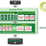
  • Implementing the program with the Atrenta IP Kit – (Mike Gianfagna, Atrenta)
  • Practical results of program participation – (John Bainbridge, Sonics)
  • Questions from the audience (10 min)

Anyone who is contemplating the use of soft IP for their next SoC project should attend this webinar, absolutely!


SoC Derivatives Made Easier

SoC Derivatives Made Easier
by Paul McLellan on 03-01-2013 at 2:44 pm

Almost no design these days is created from scratch. Typical designs can contain 500 or more IP blocks. But there is still a big difference between the first design for a new system or platform, and later designs which can be extensively based on the old design. These are known as derivatives and should be much easier to design since they can leverage not just the pre-existing IP but much of the way that it has been interconnected (not to mention much or all of the software that today forms so much of the investment in an SoC).


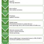
Atrenta’s GenSys is a tool that structures the whole process of doing derivative designs. It reads in an existing design in RTL (or a standard database like IP-XACT) to bring the design database into a new structured object model. This is a more reliable, flexible and just easier way to make changes according to a derivative design specification.

GenSys makes it easy to add, delete and update the existing IP blocks and their interfaces. Only a few clicks are required to remove a block or to update one. It also provides a very interactive way to build connections which can be used to update the existing connectivity with full transparency. Altering the hierarchy to group or ungroup blocks is also straightforward.

Taping out the design is also much easier. The design can be saved in interoperable formats such as IP-XACT or XML. The RTL netlist and schematics for the derivative design are then produced. The high level internal view means that it is simple to generate extensive design documentation.

GenSys is a framework for creating a derivative design while boosting productivity in terms of quick iterative cycles while eliminating errors in the design.

  • Ease of data entry
  • Fast design build time
  • Ability to accept large modern designs
  • Support for last-minute ECOs
  • Automated generation of RTL netlist, design reports and documentation
  • Customizable to support in-house methodologies
  • Standard database backend allowing API-based access

GenSys has been used to tape out many chips at leading semiconductor companies. The GenSys white paper on derivatives is here.


We Live on a Radioactive Planet

We Live on a Radioactive Planet
by Paul McLellan on 03-01-2013 at 1:45 pm

Often as we move down the process node treadmill, new challenges appear that we didn’t really have to worry about before. Often, these challenges require addressing at a number of different levels: the process, the cell libraries, the design, the EDA tools that we use.

One well known example is the problem of metal migration. If a current is too high through a metal wire that is too narrow then the current actually moves the metallic atoms creating a narrower neck, which is a positive feedback that makes the problem worse. Eventually the metal opens completely and the chip fails. We address this at many levels. At the process we design metal to be able to carry a high current (except in DRAMs where we do everything we can to keep the metal cost down). At the design level we need to make sure that we do current analysis. We need EDA tools to perform the analysis and allow us to address hot spots. Each process node typically makes the problem worse. For example, at 20nm, did you know that a large buffer is no longer in spec if it drives minimum width metal?

Another problem like this that is starting to become a real issue is soft errors caused by radiation leading to single event effects (SEE). SEE cause unpredictable system behavior and threaten safety and reliability. No surprise that this threat is increasing with smaller geometries. SEE generally occur from nuclear decay of packaging materials or atmospheric particles accelerated towards the earth by cosmic rays.


The problem needs to be addressed at multiple levels like the metal migration issue. The materials used in manufacture need to be analyzed, not just in the fab but also packaging material, bumps, solder. But we live on a radioactive planet that is bombarded with cosmic rays, so even with the best materials there is still a risk of SEE. How big a risk is affected by design of the cells (flops and memories that can be flipped into the wrong state) and by the layout of the design itself.


Just as with metal migration, which we can accelerate by raising the temperature, we can analyze product by putting it in a more radioactive environment. However, while that is great for in-depth reliability analysis, it is pretty useless for a real design where we need tools to analyze the problem before tapeout and manufacture, when we can still do something about it.

IROC Technologies is the leader in this space. They do everything from working with foundries such as TSMC and Global Foundries to analyze the whole manufacturing process, to working with fabless companies such as Qualcomm, Broadcom, Cisco, Rambus, Xilinx to help them determine whether or not they have problems and how to address them. Intel and IBM have in-house groups to do all this, but the fabless ecosystem relies pretty much on IROC for expertise in this area.

IROC can do the radiation testing and alpha particle counting. On the tool side, they have two products:

  • TFIT, a simulation tool that predicts quickly and accurately the failure rate (FIT) of cells designed for specific foundry’s technologies.
  • SOCFIT, a tool that predicts quickly and accurately the failure rate (FIT) and various derating factors of ASICs and SoCs, using either RTL or gate-level netlist

If you are a designer, especially if your designs go into products that require high reliability (medical, automotive, internet infrastructure etc) then you need to start to worry about the possibility of SEE. And memory cells are now so small that a single particle can affect more than one bit so it is critical to understand how the adjacency of different bits interacts with whatever ECC is being used to correct errors. The end customers (automotive companies, cloud infrastructure companies, router and base-station companies etc) will start to have specifications for SEE reliability which will then get driven down into the supply chain.

IROC Technologies website is here.


Modern Data Management

Modern Data Management
by Paul McLellan on 03-01-2013 at 12:17 pm

Most mixed-signal design teams don’t use data management. Well, that’s not entirely true, everyone has to do data management of some sort, it is just that it is often very ad hoc, often done by some vaguely systematic way of doing file naming, using email to keep track of changes, no access control and so on. This leads to all sorts of problems such as losing changes, running verification against the wrong cells, miscommunication. Generally, the schedule slips out as nobody really seems to know exactly what remains to be done or which the “golden” files for tapeout are.

As mixed signal designs have got larger, and as the amount of verification and characterization required is growing larger and larger with each process node, this sort of non-data-management data-management no longer cuts it. And that’s before even starting to worry about syncing data between geographically separated design teams. Or the exploding amount of disk space required since everyone feels they need their own copies of everything just to be safe.

At CDNLive on March 12th, ClioSoft will be showing their hardware configuration management tools which are seamlessly integrated with Cadence’s Virtuoso environment. It avoids all the problems above by keeping track of all the versions completely automatically.


Each user works in their own scratch environment and updates their work into a shared project repository. Each check-in creates a new version of the cell, but it can be reverted to any older version at any time. The change history (who changed what and when) is also maintained automatically. Also, unlike in the ad hoc approaches, the project administration can control who gets to do what to which cells.


For multi-site operation, there is a primary repository and then, for performance reasons, each site has a cache of the repository. Changes made at any site are automatically propagated from the primary server to all the cache servers so that all users see all changes in real time.


One thing that users need to do is to look at a version of a cell and see what was changed from either the previous version or some earlier important version (such as the last fully verified version). Since the cells are actually stored as binary files, a regular file compare program is basically useless. Visual Design Diff (VDD) allows different versions of schematics or layout to be compared graphically with the changes highlighted in Virtuoso.

Using the ClioSoft Data Management (DM) system makes the development process more structured and better controlled, both for the designers themselves and for the management team. Everyone is much more aware of what everyone else is doing, leading to shorter project schedules, fewer respins, and a lot less day to day frustration.

Details of the silicon valley CDNLive, including registration, are here.

Also Read

Cadence ♥ ClioSoft!

A Brief History of ClioSoft

Using IC Data Management Tools and Migrating Vendors


OTP based Analog Trimming and Calibration

OTP based Analog Trimming and Calibration
by Eric Esteve on 03-01-2013 at 10:16 am

Embedded NVM technology based functions can be implemented in large SoC designed in advanced technology nodes down to 28nm, as there is no requirement for extra mask levels, like when integrating Nand Flash, negatively impacting the final cost. And it is also possible to integrate One Time Programmable (OTP) to store trim and calibration settings in an analog device, usually designed in more mature technology node, so that the device powers up already calibrated for the system in which it is embedded. Variations in chip processing and packaging operations result in deviations of analog circuits and sensors from their target specifications. To optimize the performance of the systems in which these components are placed, it is necessary to “trim” interface circuitry to match a specific analog circuit or sensor. A trimming operation compensates for variations in the analog circuits and sensors due to manufacturing variances of these components.

Sidense 1T-Fuse™ technology is based on a one transistor non-volatile memory cell that does not rely on charge storage, rendering a secure cell that can not be reverse engineered. The 1T-Fuse™ is smaller than any alternative NVM IP manufactured in a standard-logic CMOS process. The OTP can be programmed in the field, during wafer or production testing.

In fact, the trimming requirement becomes more important as process nodes shrink due to the increased variability of analog circuit performance parameters at smaller processes, due to both random and systematic variations in key manufacturing steps. This manifests itself as increasing yield loss when chips with analog circuitry migrate to smaller process nodes since a larger percentage of analog blocks on a chip will not meet design specifications due to variability in process parameters and layout.

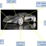
Examples where trimming is used include automotive and industrial sensors, display controllers, and power management circuits. If you look at the superb car at the top of the article, you realize that OTP technology can be implemented in several chips used to build “life critical” systems: Brake calibration, Tire pressure, Engine control or temperature or even Steering calibration… The field-programmability of Sidense’s OTP allows these trim and calibration settings to be done in-situ in the system, thus optimizing the system’s operation. Other examples where automotive trimming and calibration operations occur include secure vehicle ID (VID) storage, in-car communications, infotainment systems. The examples in the figure are for trimming and calibration of circuits such as analog amplifiers, ADCs/DACs and sensor conditioning. There are also many other uses for OTP, both in automotive and in other market segments, including microcontrollers, PMICs, and many others.

The above picture is a MEB view of the 1 Transistor OTP technologies, illustrating very interesting characteristics helping to guarantee high security level, pretty useful in SC industry today. In fact, the 1T-OTP bit-cell is very difficult to reverse engineer, as there is no difference between programmed and un-programmed bit. And, for applications requiring safe storage for secure keys, code and data, 1T-OTP macros incorporate other features for additional security, including a differential read more (no power signature), and probably a bunch of features that should be discussed face to face with Sidense!

A wide range of 1T-OTP macros are now available in many variants at process nodes from 180nm down to 28nm, and the technology has been successfully tested in 20nm. The company’s focus looking ahead is on maintaining a leadership position with NVM at advanced process nodes and solutions focused on customer requirements in the major market segments, including mobile and handheld devices, automotive, industrial control, consumer entertainment, and wired and wireless communications.

Eric Esteve from IPNEST


When the lines on the roadmap get closer together

When the lines on the roadmap get closer together
by Don Dingee on 02-28-2013 at 12:53 pm

Tech aficionados love roadmaps. The confidence a roadmap instills – whether using tangible evidence or just a good story – can be priceless. Decisions on “the next big thing”, sometimes years and a lot of uncertain advancements away, hinge on the ability of a technology marketing team to define and communicate a roadmap.

Any roadmap has three fundamental pieces: reality, probability, and fantasy. The first two, taken together, are critical to success. A good reality is better, but even a relatively dismal current product situation can be overcome, if there is some credibility left, on the strength of the probability story in the middle. (I actually created and told a crappy reality but good probability roadmap story once this way: “We took a vacation. We’re back, and here’s what we’re doing based on what we heard customers say they wanted.” It was true; we were a new marketing team with experience, and we spent a lot of time with hundreds of customers on the listening part to get the next thing we said right.) Companies that fail to execute on the probability story – the absolute must-have for customers that have bought in – risk losing credibility fast.

If both the reality and probability stories and execution hold up, attention turns to the fantasy portion. A fantasy has a lot of components: difficult enough to be interesting, achievable enough to look believable, and dramatic enough to get people excited. The fantasy part of the roadmap evolves: if successful, it becomes the probability portion, with more definition and firmer timeframes, and it gets triumphantly replaced by a new and improved fantasy. If not successful, it gets replaced anyway with a different, hopefully improved vision.

We are seeing one of the bigger roadmap marketing efforts of our time right now, weaving a story around the progression from 28nm, to 22/20nm, to 14nm and beyond.

We know 28nm processes are relatively solid now, having endured most of the transition woes in getting any process technology to volumes. We’ve been able to get a fairly good estimate of the limits of the technology, as measured by a 3GHz ARM Cortex-A9 as the consensus of the fastest core we’ll see in 28nm. Foundries are churning out parts, more and more IP is showing up, and things are relatively well.

At the other end, the industry went giddy when Altera and Intel recently announced they will work together on 14nm. There is some basis in their earlier cooperation on “Stellarton”, a primitive attempt at an Atom core and some FPGA gates in a single package. The most definite thing in this new announcement is Intel is looking to have a 14nm process up “sometime in 2014”, which is usually code for December 32[SUP]nd[/SUP], with some slack. In a best case scenario, we’d probably see an Altera part – sampled, count them, there’s one – about two years from right now.

Difficult? Yep. Billion dollar fab, new FinFETs, big chips. Achievable? Sure. If there is any way to prove out a new process, it is with memory or programmable logic, mostly uniform structures that can be replicated easily. Dramatic? A mix of people saying Altera is now ahead, Xilinx is suddenly behind, and Intel is completely transforming themselves into a leading foundry. Wow. We’ll leave the discussion on high-end FPGA volumes for another time.

What we should be discussing more is the probability story, and that lies in the area of 20nm. It is what people are actually facing in projects now, and there are some changes from the 28nm practices that are extremely important to understand. Cadence has released a new white paper “A Call to Action: How 20nm Will Change IC Design” discussing some of these ideas.


Among the changes Cadence identifies, the first is obvious: double patterning, with a good discussion of what to do about it. Another area of concern is the increasing amount of mixed-signal integration, something designers have tended to avoid. That factors into the third area, layout-dependent effects and better design rule checking. An interesting quote:

At 20nm up to 30% of device performance can be attributed to the layout “context,” that is, the neighborhood in which a device is placed.

The final discussion is on better modeling and concurrent PPA optimization, dealing with the disparities in IP blocks from many sources – 85 blocks in a typical SoC today, and growing – in the clock and power domains. This is a key part of Cadence’s approach to 28nm, and becomes even more important at 20nm and beyond.

Dealing with the probabilities will tell us more than any press release on what might be “the next big thing.” If you’re looking at what you’ll face in moving to 20nm, the Cadence white paper is a good introduction. What other design issues are you seeing in the transition from 28nm to 20nm? Am I too pessimistic on the 14nm story, or just realistic that there are a lot of difficult things to solve between here and there? Thoughts welcome.


TSMC (Lincoln) vs Samsung (Clinton) vs Intel (Washington)

TSMC (Lincoln) vs Samsung (Clinton) vs Intel (Washington)
by Daniel Nenni on 02-28-2013 at 9:00 am

Usually I sleep on long flights, if not, I watch movies and read. The Lincoln movie was playing on EVA Air this week which reminded me that Abraham Lincoln was one of the greatest U.S. Presidents. If I was asked to pick a U.S. President as a spokesperson for TSMC it would be Honest Abe Lincoln. Chairman Morris Chang said it best during his keynote, “We do not screw customers!” Samsung, on the other hand, chose Bill Clinton for their CES keynote which is also a good fit in my opinion (Clinton was impeached for lying and cheating but he is still a very popular President). For Intel I would choose George Washington, our founding father of microprocessors and GLOBALFOUNDRIES would be Barack Obama.

Associating with an American President is certainly good business since the U.S. market is the largest and Western culture is often emulated. Unfortunately honesty and decency is not always the top business priority in competitive markets so Abe Lincoln for a CES keynote would be a tough sell. Even with the incredible amount of intellectual property contained in semiconductors and consumer electronics, trust does not seem to be a prevailing factor.

Look at the Apple relationship with Foxconn. With horrible working conditions in their China factories that resulted in riots and suicides and many technology “leaks”, Apple still manufactures their all American iProducts at Foxconn. Look at Apple’s relationship with Samsung. With never ending legal actions Apple is still Samsung’s number one customer even though Samsung is Apple’s number one competitor. According to the press, Apple is moving away from Samsung but I’m not convinced it is a result of the quest for honesty and decency. From what I have learned Apple is using second source suppliers to negotiate better pricing from Samsung. The true test will be Apple’s 14nm SoC. Will Apple go back to Samsung or stay with TSMC? Apple will go back to Samsung, absolutely.

My experience at Avant! is another example. Even though the Avant! P&R tool was under indictment, customers still purchased the tool because it gave the best results making their semiconductor design faster, cheaper, more competitive. Profits over honesty and decency once again.

Sometimes our friends become our enemies, and sometimes our enemies become our friends

It is the classic tale of the scorpion and frog. A scorpion asks a frog to carry him across the water. The frog is afraid but the scorpion assures the frog that if he stings him it would be bad for both of them. The frog agrees and starts carrying the scorpion across the water but the scorpion stings the frog anyway because it is his nature. Profits are the nature of business so don’t be to surprised if you get stung by one of your friends.

Even with my bias against Samsung, my wife has informed me that we will be buying a new Samsung washer and dryer this year. She saw them at CES, they are clearly the smartest and best value, so honesty, decency, and my personal bias will not be a factor in the purchase decision. Unless of course I want to do the mountain of laundry my kids and I generate every week and I certainly do not. Laundry over ethics for sure.


Wally Rhines: Name That Graph!

Wally Rhines: Name That Graph!
by Paul McLellan on 02-27-2013 at 4:04 pm

Wally Rhines gave the keynote at DVCon yesterday. He started out with a game of “name that graph” which was unfortunately a bit spoiled since when the names were revealed the first line was off the top of the screen. But he extrapolated several trends such as the decreasing number of fabs (the current trend is that there won’t be any left by 7nm) or the number of EDA companies left for Synopsys to acquire. Or that in a few more years, designers will spend 100% of their time on verification.

But then he had some more serious graphs. Mentor had run a 3rd party survey examining trends in verification. This survey has been done under various auspices several times in the last decade. But it was done blind, nobody who participated knew it was Mentor sponsoring the survey, and by the way that the question that asked about simulators had Cadence, Mentor and Synopsys pretty much equal meant that it didn’t get biased towards Mentor’s own customers.

I’m not going to try and recap all the graphs here, but pull out a few trends that Wally highlighted. Or is that highlit?


The first trend is that standardization has gone a long way, especially around SystemVerilog which is almost universally used for large designs and is the only language that isn’t shrinking apart from a little use of C++.


Accelera UVM is also having huge growth at the expense of everything else so that there is increasing standardization of the verification flow.


One thing that is clear is that adoption of advanced verification methodologies and a structured approach to verification results in much higher productivity. The old way of buying some tools and then using them in an ad hoc way just doesn’t cut it. Verification costs go up. But groups that have a good process for verification and the tools to support it see their costs decrease.


One particular area that has a huge impact is intelligent test bench. It significantly reduces the redundancy inherent in constrained random. Last time Wally gave a keynote at DVCon he offered a deal that anyone could send him their verification suite and if he didn’t get a 10X improvement then the software was free. First design they got…improvement only 9.5X. Aargh. But every other design was much faster, some by as much as 60X.

Formal verification has also advanced. Partially this is more powerful capabilities, but also that the technique no longer requires a degree in rocket science to use it. Also, by focusing the technology on smaller applications such as connectivity or unknown analysis make formal approaches much easier to apply and with much faster run-times.

The next area Wally feels is ripe for some standardization is the system level. This is currently at the point that everyone is jockeying for position but something might emerge around transactional level models (TLM) used to drive both high level synthesis and virtual platforms for software development.

Maybe he’ll be giving the keynote again in a couple of years and be able to report how system level productivity has improved driven by standards, better processes and more powerful tools.


Shrinking audio creates issues and opportunities

Shrinking audio creates issues and opportunities
by Don Dingee on 02-26-2013 at 6:00 pm

There is a lot more to sound than meets the ear, and there a vast number of ways to deliver an audio experience. I recently trashed my gaming headset, replacing it with a Samson C03U mic and Audio-Technica ATH-PRO700MK2 headphones. It’s a huge upgrade, especially for podcasting, and I admit I was also motivated by research into digital music formats. Audio is fascinating, and I enjoy learning about how it works.
Continue reading “Shrinking audio creates issues and opportunities”