

We have frequently said in Semiwiki how crucial is it for the SC industry to benefit from high quality PHY IP… even if, from a pure business point of view (MBA minded), PHY IP business does not look so attractive. In fact, to be able to design on-the-edge SerDes and PLL (the two key pieces), you need to build and maintain a highly skilled and well experienced design team, benefiting of salaries in the top range of the industry, the EDA toolset needed to support high end analog design is also in the high range. On top of these needs to support the design phase, you also need to build a characterization lab, filled with expensive oscilloscopes able to track ps jitter and calculate BER…

Finally, because analog world is like the real world, that is, more unpredictable than the digital, the risk of redesign is far to be null! But, if you want to be able to support the ever increasing need for data bandwidth linked with the smartphone usage explosion and the requirement for accessing data in the cloud, you simply need to benefit from higher speed protocols, like 10G-Base KR or PCIe Gen-3, and to be able to create efficient systems, you need to integrate PHY supporting up to 10 Gbps data rate. A country based industry not able to design such high speed PHY IP would be like some other industries being forced to import from other countries the rare earth material absolutely essential to build key aeronautic, defense or communication systems …
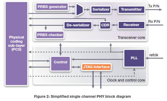
Looking at a single channel PHY block diagram makes you disappointed? You think that a PHY design does not look that complex? In fact, some of the most important features are difficult to highlight in a block diagram, like:
- Multi-featured (CTLE and DFE) receiver and transmitter equalization: adaptive equalizers have many different settings, and in order to select the right one there needs to be some measure of how well a particular equalization setting works. The result will be to improve Rx jitter tolerance, ease board layout design, and improve immunity to interferences.
- Mapping the signal eye and output the signal statistics via the shown JTAG interface: this allows for simple inspection of the actual signal. This in-situ testing method can replace very expensive test equipment (when a simple idea gives the best results!)
- The pseudo-random bit sequencer (PRBS) generator send patterns to verify the transmit serializer, output driver, and receiver circuitry through internal and external loopbacks (keep in mind that Wafer level Test equipment are limited in frequency range, such a circuitry allows running test at functional speed on a standard testers).
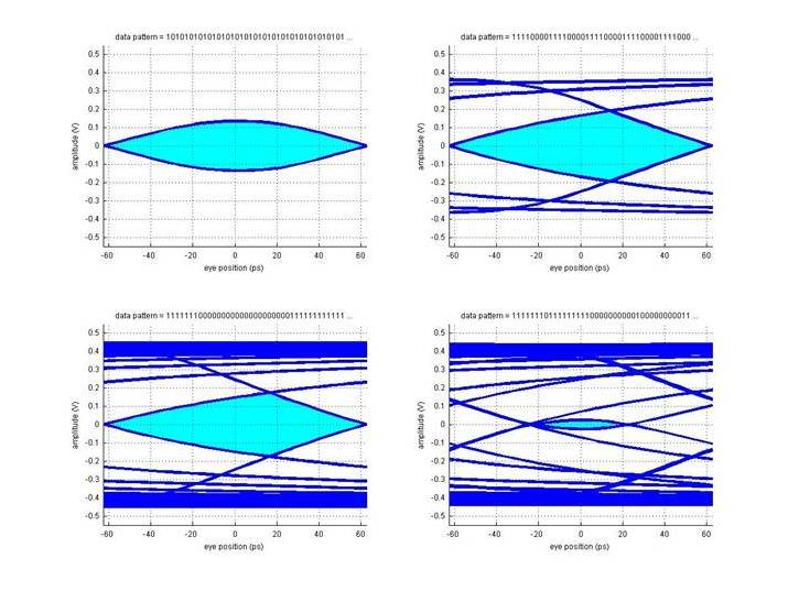
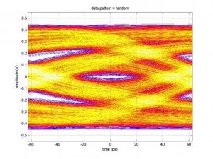
If you are interested by Eye diagram measurement, and more specifically want to know how to reduce PCI Express 3 “fuzz” with multi-tap filters, you definitely should read this blog from Navraj Nandra (Marketing Director PHY & Analog IP with Synopsys). The very didactical article explains how adaptative equalization works, Inter Symbol Interferences (ISI), as well as help to understand how signals contain different frequency content, illustrated by four examples of forty bit data patterns, from the Nyquist data (data pattern alternating 1010 data) which is the data pattern which has the highest frequency content possible to the pattern integrating 20 ’0′s followed by 20 ’1′s, which represents the signal with the lowest frequency content. Navraj has been able to explain advanced signal processing concepts by using simple words, and this is everything but simple to do!
If you just want to know what are the protocols supported by the multi-rate PHY IP spanning 1.25 Gbps to 10.3 Gbps data rates to cover key standards: PCI Express 3.0, 10GBASE-KR, 10GBASE-KX4, 1000BASE-KX, CEI-6G-SR, SGMII and QSGMII, just download the “Enterprise 10G PHY IP” datasheet here, or have a look at this PR from Synopsys…
Eric Esteve from IPNEST


Comments
There are no comments yet.
You must register or log in to view/post comments.