

I used my secret powers (being a blogger will get you a press pass) to go to the first day of the SPIE conference on advanced lithography a couple of weeks ago. Everything that happens to with process nodes seems to be driven by lithography, and everything that happens in EDA is driven by semiconductor process. It is the place to find out if people believe EUV is going to be real (lots of doubt), how about e-beam, is directed self-assembly really a thing.
The keynote was by William Siegle called Contact printing to EUV and was a history and lessons learned from a career from when lithography started to the present day (well, a little bit into the future even).
Back when ICs first started, the technology was 1X contact printing. The mask would physically be in contact with the wafer (like a contact print in photography before everything went digital). The design was actually hand-cut out of a red plastic called rubylith (originally a trademark like escalator) at 5X the actual size. This would then be photographically reduced to create the master mask. The master mask would then be used to create submaster masks. And the submaster masks used to make working masks. The working masks didn’t last very long because they were physically in contact with the wafer and so would get damaged and pick up defects fast. One lesson was to beware 1X printing.
IBM decided that the thing to do was to use the technology used to make the mask, photoreduction, to build a stepper (although I don’t know if they used that name back then). But it turned out to be much harder than they thought and the project failed. Perkin-Elmer were the first to build a successful optical projection stepper. It was still a 1X reduction, the polygons on the mask the same size as on the wafer, but the mask didn’t contact the wafer so the damage/defect problem was much reduced.
Late 1970s steppers finally make it into production. Embarrassingly for the US, Nikon and Cannon soon had better machines than GCA and PE and dominated the market by the late 1980s. In the mid-1980s ASML emerged (and absorbed PE).
The US got seriously worried about the Japanese, not just in steppers but in semiconductor memory too. Until that point there had been no co-operation among companies but that was about to change. SRC, Sematech, DOD VHSIC program, IMEC, LETI, College of nanoscale science and engineering (CNSE) at University of Albany. Another lesson was that sharing enables faster progress.
There was dramatic advances in the 1990s as we went from 365nm to 248nm to 193nm light (we are still at 193 today) along with continual improvement in the photoresist, most notably the invention of CAR (chemically amplified resist) and excimer lasers. IBM actually had all this but kept it secret until they realized that the equipment industry would never build the equipment they needed at IBM until good resist was widely available.
There were some blind alleys too. Ebeam was used in the mask shop and everyone wondered if it would make it to the production flow. The challenge with e-beam is resolution versus throughput. If the beam is small, the throughput is low. As we moved to smaller nodes, e-beam became non-competitive.
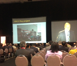
The big blind alley was X-ray lithography (around 1nm wavelength). This was killed by three things. Firstly, it needed a synchrotron as a source of X-rays. Second, it required a 1X membrane mask. And remember, beware of 1X printing. But mostly it was built on a false assumption that we would not be able to get beyond 0.25um using optical technology. Well, we are pretty much at 14nm using that technology which is 0.014um in old currency. So one more lesson was to never underestimate the extendability of existing technology.
What has enabled light to last so long was a combination of optimizing the mask (optical proximity correction, OPC) and holistic litho optimization.
There are also promising future technologies. Nano-imprint has remarkable image fidelity (where the mask essentially is pressed onto the wafer). But it has all the same problems as the rubylith era, of 1X contact printing meaning that masters, submasters and working masks are required.
Of course the big hope for the future is EUV with a wavelength of 13.5nm with a 4X reduction reflective reticle. But we need to get the light source power up to 100-250W, we need production worthy masks, resists and metrology. The justification is economic, to avoid multiple patterning, but that it won’t be adopted until it can beat that cost ceiling.
And the future? Another rule, it is impossible to predict 10 years ahead. So at this point we can’t tell if EUV will make it, if directed self-assembly will turn out to be a breakthrough, if carbon nanotubes can be manufactured into circuits economically. We can really only see out about 3 years.


TSMC CoWoS versus Intel EMIB Semiconductor Packaging