The design of parallel interfaces is supposed to be (comparatively) easy — e.g., follow a few printed circuit board routing guidelines; pay attention to data/clock/strobe signal lengths and shielding; ensure good current return paths (avoid discontinuities); match the terminating resistances to the PCB trace impedance; and provide good decoupling capacitance, especially on the signal termination reference voltage. The definition of the DDR4 interface standard by JEDEC incorporates many new features beyond DDR3, and requires that designers place additional focus on the “data eye” analysis that has primarily been the domain of SerDes serial interface implementations.
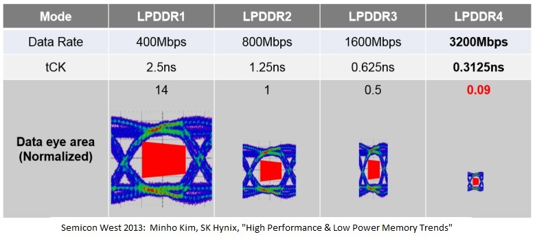
At DDR4 data rates, the validation of data “DQ” signaling is transitioning from setup/hold timing checks to a true eye margin analysis. The figure below illustrates a rather startling trend in the (LP)DDRn standard, in terms of the available eye opening.
This article highlights but a few of the new features of the DDR4 standard and the corresponding analysis and verification challenges.
I recently had the opportunity to chat with Nitin Bhagwath, technical marketing engineer at Mentor Graphics, who provided me with a great overview of DDR4. [ Nitin: A belated “Thanks!” ]
The motivations for the DRR4 standard are much broader than simply increasing memory bandwidth, although that’s certainly still the “prime directive”. The VDDQ supply has been lowered from 1.5V for DDR3 to 1.2V, to save power. Specific features have also been included to enable additional power and simultaneous switching noise optimizations.
Vref /= VDDQ/2
The biggest change from DDR3 is the adoption of a new on-die termination (ODT) approach, which results in a significant change in the DQ switching threshold voltage.
As illustrated below, DDR3 used a receiver termination impedance to VDDQ/2. Conversely, DDR4 uses a VDDQ pullup termination — aka, “pseudo-open drain” or “POD1.2“.
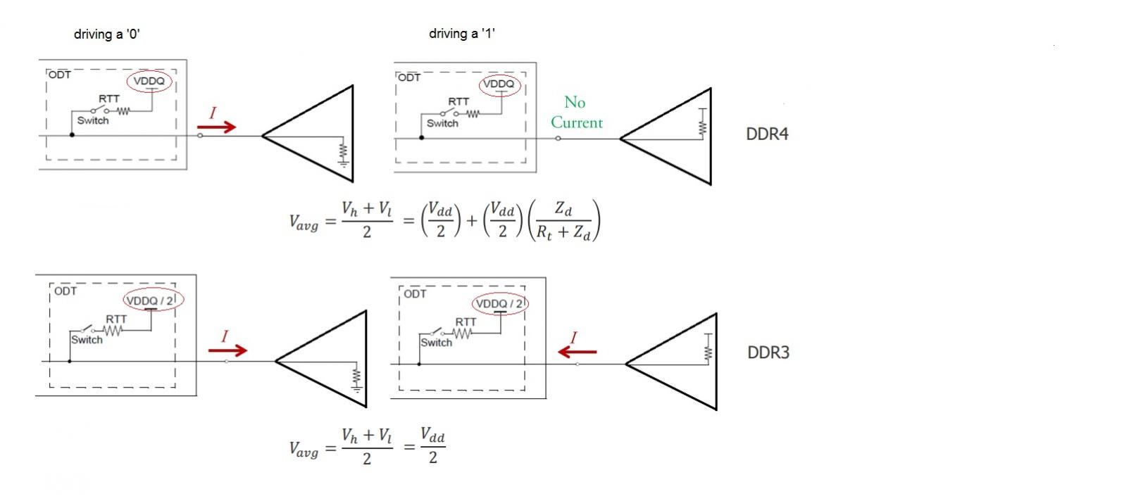 As a result, the average voltage levels between ‘1’ and ‘0’ are VDDQ/2 for DDR3 — the reference voltage used as the data threshold is available with a straightforward voltage divider, using two equal (low tolerance) resistors.
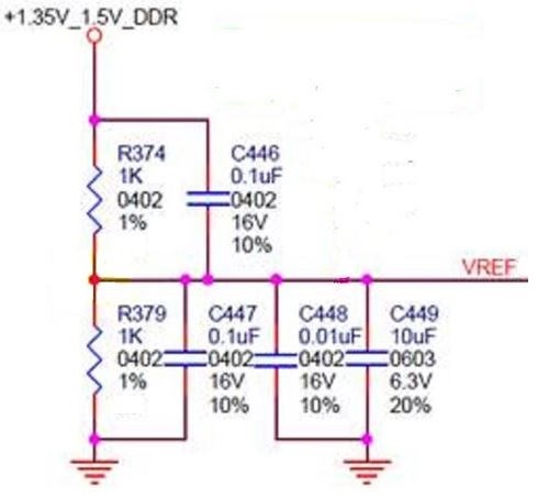
For DDR4, however, the average voltage levels are above VDDQ/2, based upon the driver impedance and receiver termination resistances — the center of the data eye is shifted upwards from VDDQ/2.
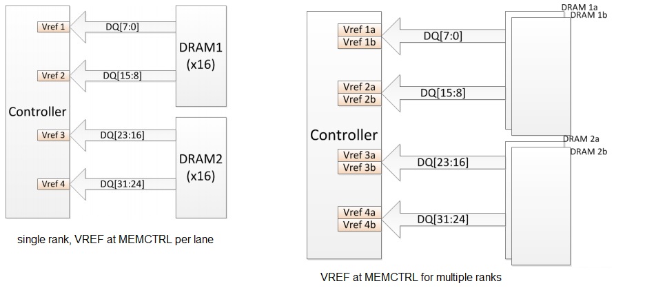
As there will be variation from pin-to-pin in the on-die receiver termination and driver resistances at both the MEMCTRL and DRAM‘s, the expected voltage range between ’1’ and ’0’ will have pin-to-pin tolerance, as well. Therefore, a key DDR4 design implementation requirement is the “training” of a programmable internally-generated switching reference. This reference voltage will be determined during an initialization sequence performed by the MEMCTRL, typically using one reference per data lane at the controller and one reference for the DRAM.
(Note: The termination to VDD for DDR4 DQ signals is similar to the GDDR5 interface. Also, the DDR4 address/command signals continue to use the termination resistor connected to VDDQ/2, and an external VREF.)
Power Optimizations in DDR4
Why change the DDR4 termination from DDR3? Current is flowing between the MEMCTRL and DRAM for either a driven ‘1’ or ‘0’ DQ signal in DDR3, whereas in DDR4, current is only present for a logical ‘0’ signal — the VDDQ termination results in no current for a logical ‘1’. Significant power savings is achievable if the DQ data bit values transferred between the MEMCTRL and DRAM could be biased toward a higher percentage of 1’s. The aggregate simultaneous switching noise (SSN) of successive data bursts will be reduced, as well.
DDR4 adds a Data Bus Inversion signal option. A pre-calculation of the data is made, and either the true or inverted values are sent across the DDR interface to maximize the number of 1’s. The DBI signal accompanying the data indicates whether the receiver should/should not invert the incoming values when capturing. There’s a tradeoff, to be sure — designers need a tool to help assess whether the additional overhead of the DBI signaling is a significant power/SSN benefit.
Signal Integrity Optimizations in DDR4
The use of multiple ranks of DRAM on the DDR4 interface requires additional options for selecting the on-die terminating resistance for individual ranks. (A memory “rank” is defined as a set of DRAM parts sharing the same select/enable signal, which operate together in response to a command from the MEMCTRL. The overall memory architecture may divide the total capacity into multiple ranks; the additional signaling complexity is offset by opportunities for faster, interleaved read/write accesses.)
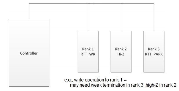
A DDR4 DRAM offers a range of terminating resistance values. The specific DQ pin receiver resistance presented to the interface is selected by a combination of the initial chip configuration and the DRAM operating command, if dynamic on-die termination is enabled. For example, during a DRAM write operation, a transition to the RTT_WR terminating resistance can be enabled. During other operations, two additional settings are available (RTT_NOM and RTT_PARK) to allow optimum signal integrity response among different ranks. The figure below illustrates an example of a write operation where different termination is used across three ranks — RTT_WR (active rank), RTT_NOM = high-Z, and RTT_PARK.
As DDR4 is approaching the complexity of a SerDes interface, I asked Nitin about the statistical bit-error rate (BER) associated with eye diagram analysis. The JEDEC spec for DDR4 defines the data eye window as requiring a BER of 1E-16 from signal integrity simulation. Nitin added that the DDR4 standard includes additional features to enhance reliability (at the expense of additional latency):
- a full cyclic-redundancy check on the DQ interface for a DRAM write operation
- parity checking on the address and command signals
If enabled, the CRC is sent by the MEMCTRL after the write data, and verified by the DRAM. There are still Error Correcting Code and non-ECC DDR4 DIMM’s — the CRC implementation goes beyond the scope of the ECC offering, as illustrated below:

The validation of a DDR4 design clearly requires a detailed SerDes-like extraction and simulation to confirm the data eye margins. Unlike a SerDes serial interface with clock-data recovery, SI analysis for DDR4 requires detailed extraction of the differential clock and data strobe signals, as well. Address and command signal validation still uses traditional setup/hold timing verification.
Nitin highlighted how the Mentor Hyperlynx v9.2 development team has enhanced the “DDR Wizard” application, to support the complex configuration options available in DDR4, and how to apply those options when selecting IBIS model parameters, running simulations, and analyzing results. Additionally, DDR Wizard features ensure that simulations will include the requisite JEDEC checks.
This guidance is absolutely required, to ensure this complex interface is thoroughly verified, while offering insight into the tradeoffs of the new power and SI optimization features available in the DDR4 standard. More information on the Hyperlynx DDR Wizard is available here; there’s an exceptional YouTube video demonstration here.
-chipguy
Share this post via:


Comments
There are no comments yet.
You must register or log in to view/post comments.