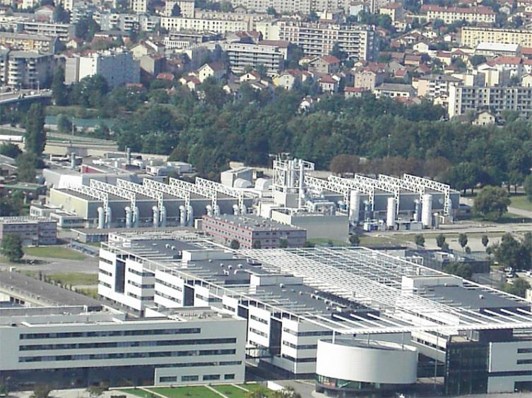
 One of the presenters at the standing-room only litho session at Semicon this week was Serge Tedesco, the litho program manager at CEA-Leti in Grenoble France. He is running a program called IMAGINE for maskless lithography. Chips today are built using a reticle (containing the pattern for that layer of the chip) which is exposed one die at a time with a flash of light, and then the wafer is moved to the next die and the process is repeated. The nice thing about this process is that the whole of each die is basically processed in parallel with that flash of light (although obviously it is a serial process to get from die to die).
Direct write e-beam takes a different approach. The e-beam is steered across the design and writes the pattern as it goes, in much the same way as a cathode-ray tube (CRT) black and white television worked, but with a rather greater resolution. A TV has dots at around a millimeter and we need dots around 20nm. So more like a scanning electron microscope. The big problem with this approach is that it is serial. No matter how fast the ebeam scans, there are a lot of points at 20nm resolution for a 300mm wafer (if I did the calculation right, about 10[SUP]15[/SUP] points). So to be effective, direct write e-beam needs more than one beam. A lot more.
The IMAGINE program started with a pre-alpha e-beam machine which could only expose 1.5mm at a rate of 0.002 wafers per hour with a single beam. The current version (beta?) has 110 beams and the next machine will have 13,260 and will have full 300mm wafer coverage and process 10 wafers per hour.
The big problems with the approach are:
- Throughput. If this is going to be viable it it needs to be cost competive with mask-based technologies. The speed of writing depends on the capabilities of the machine but also on the sensitivity of the photoresist.
- Stitching/overlay. Aligning the pattern on one layer onto the patterns already manufactured on the wafer, and given that this is wafer-scale technology then this needs to be continuously aligned, and making sure all the beams stay aligned with each other so that adjacent patterns line up.
- Data handling. Obviously the mask data (I’ll continue to call it mask data even though there are no masks) doesn’t need to be stored fully rasterized, but as the machine processes a wafer the computing infrastructure needs to transmit around 10[SUP]15[/SUP] bits of data. At a target speed, for a single machine, of 10 wafers per hour, that is something like 10 terabits per second.
- Data Integrity. A single bit wrong in the data is enough to cause a “defect”
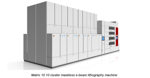
 A full machine will have a cluster of 10 wafer handling units for a throughput of 100 wafers per hour (and 130K beams). That’s a lot of beams and a lot of data handling. Apparently over half the cost of the machine is, in fact, the data handing which is transmitted to the e-beam machine itself over optical fiber.
E-beam direct write for commercial semiconductor manufacturing was actually tried in the mid-1980s. European Silicon Structures (ES2) near Aix-en-Provence (also in France) using Perkin-Elmer equipment. I know a bit about it since they tried to recruit me to work on the EDA software they knew they would need but in the end I stayed with VLSI and went and opened an R&D center for them in Sophia-Antipolis, a couple of hours east. They never got the technology to work and eventually they shut down. The software group largely went to Cadence, I think. Robin Saxby, who I think ran sales, went on to spin ARM out of Acorn and so to fame and fortune.
Share this post via:


Comments
0 Replies to “Direct Write E-beam”
You must register or log in to view/post comments.