From initial process technology development (TD) to high volume manufacturing (HVM) status for a new node, one of the key support functions to improve and maintain yield is the in-line wafer inspection technology. Actually, there are multiple inspection technologies commonly employed, with tradeoffs in pixel resolution,… Read More
Prioritizing gender-related behavior in the analysis of transportation patterns may change planning priorities and accelerate a transition to more sustainable mobility solutions. That is the finding of a report compiled by the Ministry of Environmental Protection in Tel Aviv, Israel and shared at the Women in Mobility summit… Read More
Dan is joined by Bob Smith, executive director of the ESD Alliance, a SEMI technology community. The ESD Alliance represents the electronic system and semiconductor design ecosystems. It is the first design-oriented community in SEMI.
Bob explores the mission of the ESD Alliance and how the organization leverages the worldwide… Read More
There is no shortage of reporting on the many technological advances happening within the semiconductor industry. But sometimes it feels like we hear less in the area of semiconductor manufacturing equipment than in the design and product arenas. That doesn’t mean that there is less happening there or what is happening there … Read More
The quest for bigger FPGA-based prototyping platforms continues, in lockstep with each new generation of faster, higher capacity FPGAs. The arrival of the Xilinx Virtex UltraScale+ VU19P FPGA takes capacity to new levels and adds transceiver and I/O bandwidth. When these slot into S2C’s Prodigy S7-19P Logic System, the result… Read More
“Inverse lithography technology (ILT) represents the most significant EDA advance in the last two decades.” Danping Peng from TSMC made that assertion at the recent SPIE Advanced Lithography + Patterning Conference, in his talk entitled: ILT for HVM: History, Present, and Future. This article summarizes the highlights… Read More
The capacity and energy efficiency challenges from the growing appetite for high-speed data along with advanced applications such as LIDAR and quantum computing are driving demand for increasingly large-scale photonic integrated circuits (PIC). With an ever-increasing number of components on a single photonic chip, manual… Read More
It has been an article of faith that you can’t use formal tools to validate datapath logic (math components). Formal is for control logic, not datapath, we now realize. We understood the reason – wide inputs (32-bit, 64-bit or more) fed through a multiplier deliver eye-watering state space sizes. State space explosions also happen… Read More
After many years of hesitancy to jump with both feet in, semiconductor companies are seriously considering implementing cloud strategies and making required investments. Their concern though is, how much investment is it going to take? Some of the block-and-tackle challenges they face in implementing a cloud strategy are … Read More
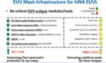
At the recent SPIE Advanced Lithography + Patterning Conference, Mark Phillips from Intel gave an insightful update on the status of the introduction of the 0.55 high numerical aperture extreme ultraviolet lithography technology. Mark went so far as to assert that the development progress toward high-NA EUV would support … Read More







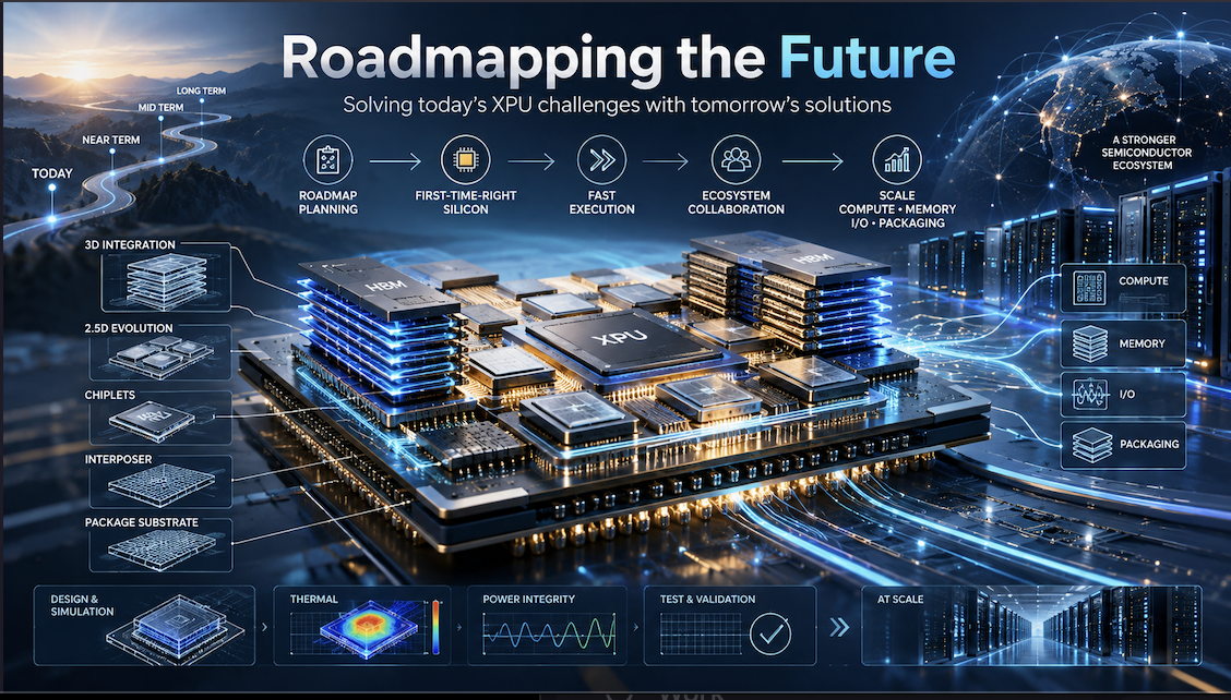






Intel Foundry: AI performance now depends on the whole system