
Semiconductor technology is among the most complex of technologies and the semiconductor industry is among the most demanding of industries. Yet the ecosystem has delivered incredible advances over the last six decades from which the world has benefitted tremendously. Yes, of course, the markets want that break-neck speed of advances to continue. But the industry is facing not only technological challenges but also a projected shortage of skilled engineers to contend with. In terms of technology complexity, we have entered the SysMoore era. The power, performance and area (PPA) requirements of SysMoore era applications are lot more demanding than the Moore’s era applications. In terms of engineering talent shortage, the demand for US-based design workers alone is expected to be 89,000 by 2030 with a projected shortfall of 23,000. [Source: BCG Analysis]
Artificial Intelligence (AI) to the rescue. With foresight, many companies within the ecosystem have started leveraging AI in their tools offerings with tangible benefits accruing to their customers. AI techniques can automate several time-consuming and repetitive tasks in the chip design process, such as layout optimization, verification, and testing. They can help automate the design process, reduce design time, and optimize power, performance, and area (PPA) tradeoffs.
Two years ago, Synopsys launched their AI-driven design space optimization (DSO.ai) capability. Since then, DSO.ai has boosted designer productivity and been leveraged for 160 production tape-outs to date. DSO.ai uses machine learning techniques to explore the design space and identify optimal solutions that meet the designer’s PPA targets. But DSO.ai capability was just the tip of the ice berg in terms of AI-driven technology offering from Synopsys. The company has been investing heavily in AI to enhance and expand their tools offerings.
Synopsys.ai
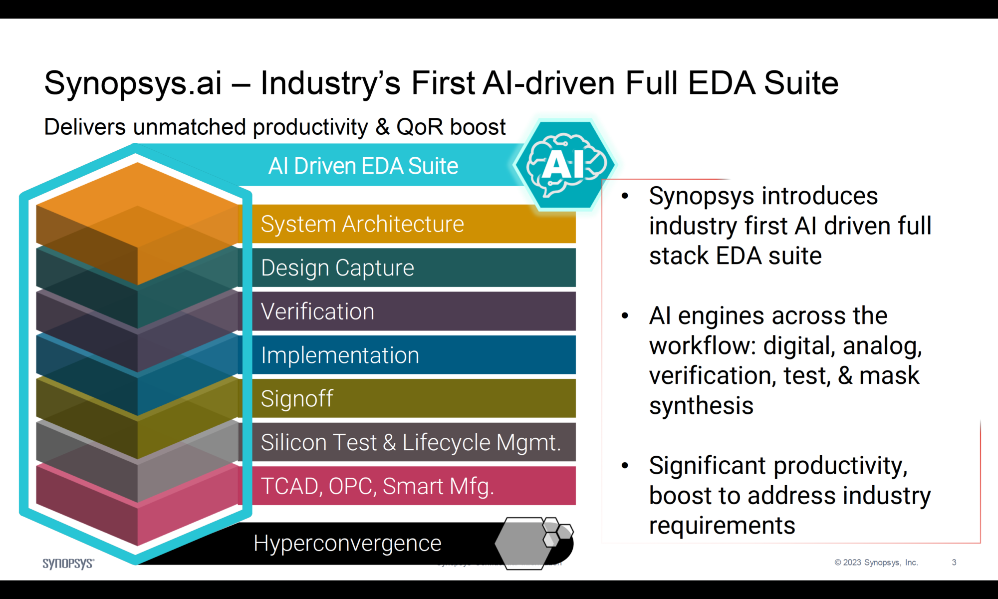
This week at the Synopsys Users Group (SNUG) conference, the company unveiled Synopsys.ai as the industry’s first full-stack, AI-driven EDA suite for chipmakers. The full suite addresses the areas from system architecture to silicon test and more.

Verification and Test
Going to market in a rapid and cost-effective manner with a chip that is high-yielding involves more than just the design implementation. The entire process of moving from architecture to design implementation to a production worthy manufactured chip can be broadly divided into Design, Verification and Test. Without successful verification, we may end up with a functionally wrong chip. Without successful testing, we may end up with a functionally failing chip. Just as the design phase is time/effort intensive, verification and testing phases are too.
AI can help verify and validate the chip design by analyzing and predicting potential design issues and errors. It can help reduce the need for manual verification and testing and improve the chip’s quality and reliability.
Verification Space Optimization (VSO.ai)
The Synopsys.ai EDA suite includes AI-driven functional verification (VSO.ai) capability. VSO.ai helps in early design validation by analyzing and verifying the chip design against the design specification and requirements. Design flaws that creeped in during the specification to design phase are identified early in the project, reducing the time and cost of design iteration further down the line.
The tool infers needed coverage from the stimulus and RTL and defines the coverage requirement. Advanced root cause analysis is performed to identify unreachable coverage. A ML-based Solver targets hard to hit coverage for higher coverage closure. A built-in regression optimizer ensures that the highest ROI tests are run first.
The end result, regression runs that take days to reach target coverage take only hours to reach and exceed the target coverage.

Test Space Optimization (TSO.ai)
The number of states in which a modern-day chip can operate is almost infinite. Looking for potential failure modes in complex chips is like searching for a needle in a haystack. This makes the task too enormous for engineers to identify these failure modes. The Synopsys.ai suite includes AI-driven silicon test (TSO.ai) capability. AI models analyze the chip design data and identify input conditions that could cause a chip to misbehave. The tool then uses these input conditions to generate test cases that exercise the chip’s functionality in an efficient and thorough manner. AI models can also suggest solutions based on root causes they identify for faults observed.

Manufacturing Lithography
Beyond arriving at a functional chip, there is also the requirement of high yielding chip for profitable volume production. The Synopsys.ai EDA suite includes AI-driven manufacturing solutions to accelerate the development of high accuracy lithography models for optical proximity correction (OPC). At advanced process nodes, OPC is imperative for achieving high yield during silicon fabrication. At this time, Synopsys is working with IBM to offer AI-driven mask synthesis solutions. It is reasonable to expect more capabilities in this area will be added to the Synopsys.ai suite over time.
Migrating Analog Designs to a Different Process
Compared to digital design, analog design has always been considered more challenging. At the same time, the pool of analog engineers has been shrinking over time. Analog design migration is a task that requires highly skilled analog engineers who are intimately knowledgeable in related process technologies. Synopsys’ AI-driven analog design migration flow enables efficient re-use of designs that need to be migrated from one TSMC process to another.
You can read the Synopsys.ai press announcement here. To learn more details, visit Synopsys.ai.
Also Read:
Power Delivery Network Analysis in DRAM Design
Intel Keynote on Formal a Mind-Stretcher
Multi-Die Systems Key to Next Wave of Systems Innovations
Share this post via:


Comments
One Reply to “Full-Stack, AI-driven EDA Suite for Chipmakers”
You must register or log in to view/post comments.