
My IC design career started out with DRAM design back in 1978, so I’ve kept an eye on the developments in this area of memory design to note the design challenges, process updates and innovations along the way. Synopsys hosted a memory technology symposium in November 2022, and I had a chance to watch a presentation from SK hynix engineers, Tae-Jun Lee and Bong-Gil Kang. DRAM chips have reached high capacity and fast data rates of 9.6 gigabits per second, like the recent LPDDDR5T announcement on January 25th. Data rates can be limited by the integrity of the Power Delivery Network (PDN), yet analyzing a full-chip DRAM with PDN will slow simulation times down too much.
The peak memory bandwidth per x64 channels has shown steady growth across several generations:
- DDR1, 3.2 GB/s at 2.5V supply
- DDR2, 6.4 GB/s at 1.8V supply
- DDR3, 12.8 GB/s at 1.5V supply
- DDR4, 25.6 GB/s at 1.2V supply
- DDR5, 51.2 GB/s at 1.1V supply
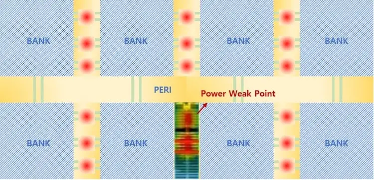
A big challenge in meeting these aggressive timing goals is controlling the parasitic IR drop issues caused during the IC layout of the DRAM array, and shown below is a plot of IR drop where the Red color is an area of highest voltage drop, which in turn slows the performance of the memory.

The extracted parasitics for an IC are saved in a SPF file format, and adding these parasitics for the PDN to a SPICE netlist causes the circuit simulator to slow down by a factor of 64X, while the number of parasitic RC elements added by the PDN is 3.7X more than just signal parasitics.
At SK hynix they came up with a pragmatic approach to reduce the simulation run times when using the PrimeSim™ Pro circuit simulator on SPF netlists including the PDN by using three techniques:
- Partitioning of the netlist between Power and other Signals
- Reduction of RC elements in the PDN
- Controlling simulation event tolerance
PrimeSim Pro uses partitioning to divide up the netlist based upon connectivity, and by default the PDN and other signals would combine to form very large partitions, which in turn slowed down simulation times too much. Here’s what the largest partition looked like with default simulator settings:

An option in PrimeSim Pro (primesim_pwrblock) was used to cut down the size of the largest partition, separating the PDN from other signals.

The extracted PDN in SPF format had too many RC elements, which slowed down circuit simulation run times, so an option called primesim_postl_rcred was used to reduce the RC network, while at the same time preserving accuracy. The RC reduction option was able to decrease the number of RC elements by up to 73.9%.
Circuit simulators like PrimeSim Pro use matrix math to solve for current and voltages in the netlist partitions, so runtime is directly related to matrix size and how often a voltage change requires recalculation. The simulator option primesim_evtgrid_for_pdn was used, and it reduces the number of times a matrix needs to be solved whenever there are small voltage changes in the PDN. The chart below shown in purple has an X at each point in time when matrix solving in the PDN was required by default, then shown in white are triangles at each point in time that matrix solving is used with the simulator option. The white triangles happen much less frequently than the purple X’s, enabling faster simulation speeds.

A final PrimeSim simulator option used to reduce runtimes was primesim_pdn_event_control=a:b, and it works by applying an ideal power source for a:b, resulting in fewer matrix calculation for the PDN.
The simulation runtime improvements by using all of the PrimeSim options combined was a 5.2X speed-up.
Summary
Engineers at SK hynix have been using both the FineSim and PrimeSim circuit simulators for analysis in their memory chip designs. Using four options in PrimeSim Pro have provided sufficient speed improvements to allow full-chip PDN analysis with SPF parasitics included. I expect that Synopsys will continue to innovate and improve their circuit simulator family in order to meet the growing challenges of memory chip and other IC design styles.
Related Blogs
-
4 Ways that Digital Techniques Can Speed Up Memory Design and Verification
-
Shifting Left with Machine Learning to Avoid 4 Key Memory Development Bottlenecks
-
Why Memory Design Technology Co-Optimization Is Key to Memory Design Success


Comments
There are no comments yet.
You must register or log in to view/post comments.