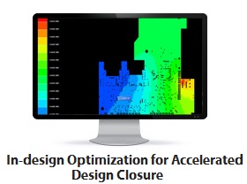
A common SoC design methodology in current use starts with preparation of the physical floorplan — e.g., block/pin placement, global clock domain and bus signal planning, developing the global/local power distribution (and dynamic power domain management techniques). Decoupling capacitor estimated densities and insertion methods are defined. From this initial plan, individual IP block implementations are pursued, using margins for local power voltage drop and dynamic noise. As the IP evolves, updates to the floorplan are made, based upon improved insights on block area, pin locations, global routing demand, etc. A key milestone is the first integration of the IP into a full-chip model.
Electrical analysis is now undertaken on the integrated model to investigate global issues, utilizing functional activity operating mode (and mode switching) patterns:
- (dynamic and static) I*R drop on power/gnd nets
- thermal mapping (e.g., identification of hot spots, generation of self-heating data)
- electromigration
The chip integration engineering team is often faced with a dilemma. The dataset size of the full-chip parasitic model is large, and increasing with each new process node. The compute resources required to perform these analyses are demanding — with current tool algorithms, a single “integration server” in the data center (with maximum memory installed) is drained of other jobs and allocated to the task. The runtime for these analyses is typically several days each — the design version snapshot used is likely already out-of-date before the jobs complete, necessitating a version sync-up/merge to effect any requisite changes from the analysis results.
The final integration is intended to provide tapeout sign-off quality results. The design database is frozen, with only judiciously-selected ECO’s allowed. Ideally, issues from prior full-chip electrical analyses have been resolved, but inevitably the convergence of late functional bug fixes, timing closure updates, and power dissipation optimizations will require a final, detailed sign-off analysis. Again, the demand for integration server compute resources — and, especially, the overall throughput for any ECO iterations — will be extreme. The sign-off DRC/DFM/DFY jobs running concurrently on the frozen database add to the compute demand pressures.
In the future, this path to sign-off will become increasingly difficult, if not intractable. The trends in parasitic dataset size, the server memory constraints, and the analysis throughput requirements are all asserting pressure on this flow. Methods to compress the parasitic network model may assist with the resources required, at a potential loss of accuracy. With the requirement to reduce supply voltage and power dissipation, and with the greater electromigration and thermal challenges of advanced process nodes, the accuracy demands are even more stringent. Alternatively, to save resources, the integration engineer could opt to skip some of the operating modes where dynamic analysis is performed. Yet, the application requirements of an increasingly diverse set of markets demand more comprehensive analysis coverage, not less (e.g., automotive, medical and healthcare, mil/aero). Clearly, the SoC design industry is at a crossroads.
I recently had the opportunity to review these concerns with Aveek Sarker, VP Sales and Support, and Ravi Ravikumar, Senior Marketing Manager, with the Semiconductor Business Unit at Ansys. Their enthusiasm for a new Ansys product strategy and emerging tools was contagious.
Ansys recently announced the SeaScapeplatform for electrical analysis tool development. Aveek said, “The big data analytics industry has addressed how to distribute, or shard, large datasets across many individual cores, each with a relatively small amount of local memory. The programming models are in place to apply map/reduce algorithms to this distributed dataset, collecting final results. We have leveraged this model, and the technology developed by a recent Ansys acquisition, Gear Design Solutions, to apply these techniques to full-chip electrical analysis. We know that future designs will require an analysis architecture that is extremely scalable. We are already seeing models approaching 10TB in size.”
The domain of chip electrical analysis is more complex than executing an SQL query on a big data model. Ansys had to develop new solvers — e.g., a distributed graph solver, a full distributed matrix solver, and data allocation methods to both fit within the allocated memory per core while minimizing inter-machine communications. And, whereas big data analytic results are typically numerical, SoC electrical analysis requires visual insights and feedback — Ansys also developed a thin client viewer to this distributed database.

SeaScape will be the application development platform for a set of multi-domain, multi-physics solutions from Ansys. The first product application available on this platform is SeaHawk, the distributed equivalent to the industry-leading RedHawk for SoC power distribution analysis.
It was at this point in our discussion where Aveek really challenged my way of thinking about chip integration and signoff — he posed the following provoking questions. “Using your existing IT data center and grid infrastructure, what if full-chip electrical analysis was completed in hours, rather than days? As an example, a 16nm SoC design from an early SeaHawk customer with 1B model elements recently completed full static and transient power distribution analysis in 5 hours.”
He continued, “What if integration engineers and unit/core implementation engineers had a much tighter optimization loop between them? Other early customers have provided feedback that they are able to more easily optimize the power distribution, no longer imposing a conservative, uniform global grid pushed down from the initial floorplan using conservative margins for the voltage drop budget. Their result was a reduction in die area.”
There is definitely a requirement to address the growing complexity of full-chip electrical (and thermal) models, while maintaining accurate analysis and efficient throughput. Ansys has adapted the infrastructure developed for big data analytics to build a distributed database management system for electronic application development, to address this demand.
More than that, however, Aveek said, “We feel we have the capability to re-invent sign-off.” If the arduous, multi-day task of full-chip electrical analysis is reduced to an optimization loop that can be run regularly on the integration model, final electrical signoff could be greatly simplified. He may indeed be right.
Please follow these links for more information onSeaScapeand SeaHawk.
If you will be attending DAC 2016, please explore the Ansys DAC presentations on this new platform and product — more information on the Ansys DAC program is available here.
-chipguy
Related Blog: Rebooting EDA
Share this post via:


Comments
There are no comments yet.
You must register or log in to view/post comments.