For years, there have been rather distinct domains for the extraction of interconnect models from physical design data.
Chip designers commonly focused on RC parasitics for circuit/path delay calculations and dynamic I*R voltage drop analysis. The annotation of extracted parasitics to a netlist model required the layout topology to be LVS-clean. For a select class of high-frequency designs with fast clock slew rates and high switching activity, the impact of inductive impedance was incorporated into the power grid and global clock model extraction. [1]
On-chip inductive spiral components utilized unique methods for electrical model generation. The layout of these components often required specific metal fill layout topologies below the (thick) top-level metals all the way down to the substrate, to simplify the assumptions about the induced current flow, as depicted below.


The package and printed circuit board design domain requires accurate RCLK model extraction, to provide the power/ground distribution impedance model and signal interconnect insertion/reflection/crosstalk losses between transceivers. The budget for allowable P/G distribution voltage level swings is inevitably very aggressive, and the cost/area tradeoffs for the addition of decoupling capacitance necessitate very detailed models. The requirement for very high datarate signaling (especially over long-reach serial interfaces) demands accurate extracted models, valid over a wide frequency range – i.e., to multiple harmonics of the fundamental datarate.
There are several technology trends that are driving new developments in these two extraction domains:
- increasing use of inductive elements on-die, placed over circuitry
The utilization of tuned RLC “tank” circuits is growing, as part of the on-die clock synthesis requirements. Wireless opportunities are expanding. The design of local oscillators as the clock source for high-speed wireline interface links between chips is using LC resonant tanks to a greater degree.

The die area allocated to these circuits is a growing concern. As illustrated in the figure above, on-die inductors are increasingly being merged with underlying circuitry, necessitating enhanced approaches to model extraction.

- advanced multi-die 2.5D and 3D packaging technologies introduce new topologies to model
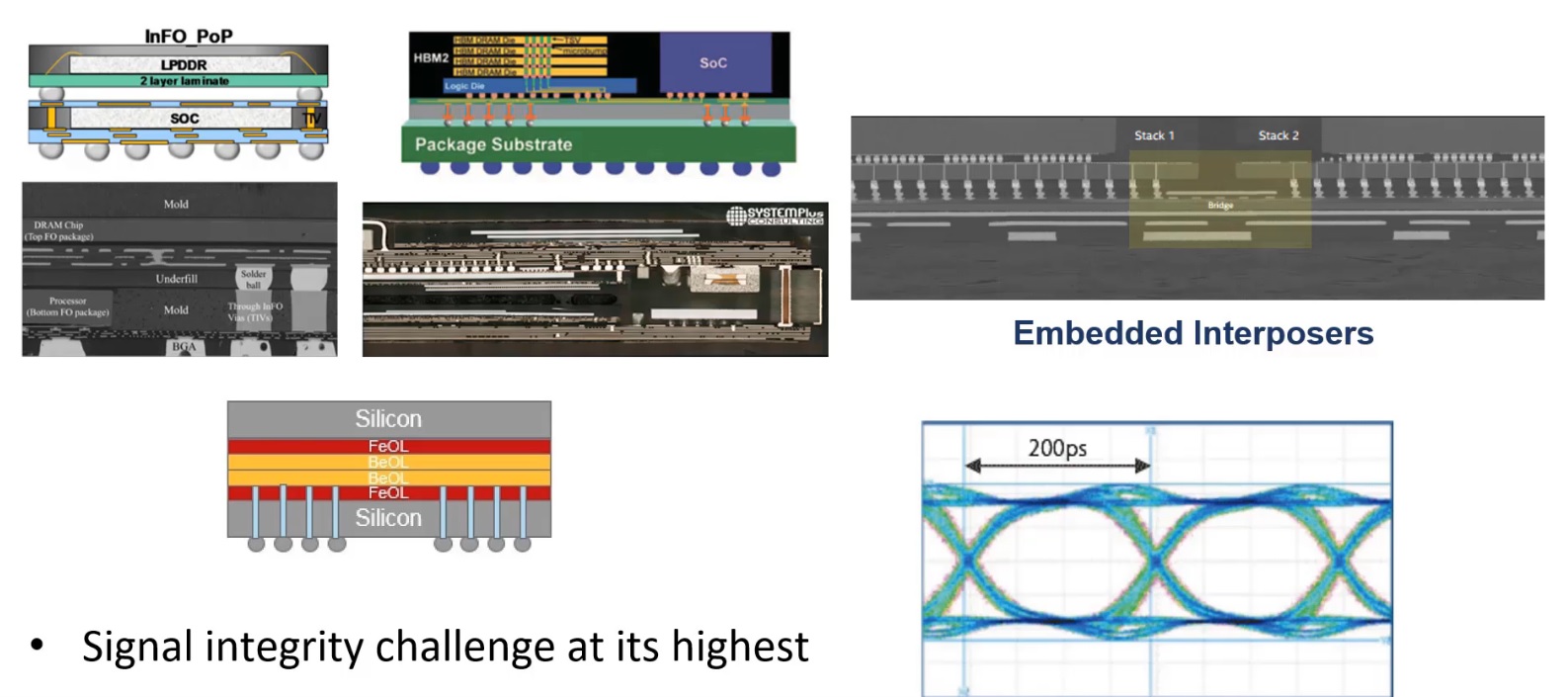
Current packaging technologies incorporate:
- TSVs for power delivery and signal connectivity from bumps to die, through stacked die
- short-reach (parallel, clock-forwarded) interfaces between die
- local redistribution interconnect layers in an interposer


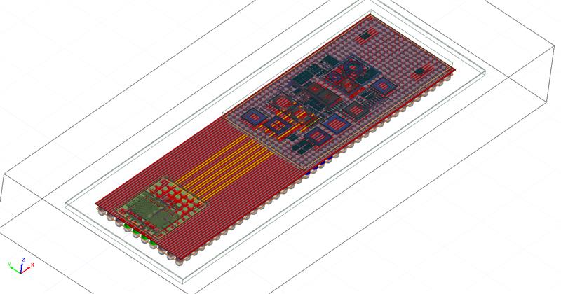
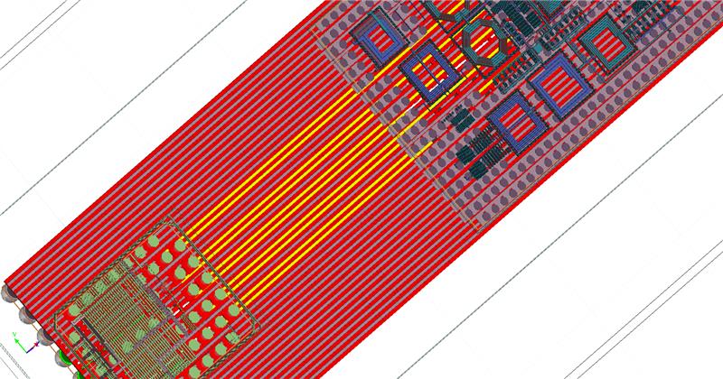
The figures above illustrate a simple 2.5D interposer structure with two die – clock lines are highlighted in yellow, as an example. It is necessary to analyze electromagnetic (EM) effects throughout the entire structure.
and, last, but most certainly not least:
- the physical design data volume associated with advanced process node die and multi-die packages is immense
The algorithms for extracting parasitic models need to support distributed computation, with highly scalable performance across multiple processor cores.
I recently had the opportunity to chat with Yorgos Koutsoyannopoulos and Anand Raman at Ansys, to get their perspectives on the trends and tool features needed to support the evolution of these model extraction domains. Their insights were most illuminating – specifically, how the recently-introduced Ansys RaptorH product addresses these evolving requirements comprehensively.
Yorgos began by saying, “The application space for RLCK extraction and simulation is expanding rapidly. The designers of 2.5D and 3D ICs are familiar with silicon-centric flows. They need a modeling solution that combines usability features with the accuracy demanded by the high signal datarates and power delivery challenges of these package solutions.”
“How did you approach that balance, between usability and accuracy?”, I asked.
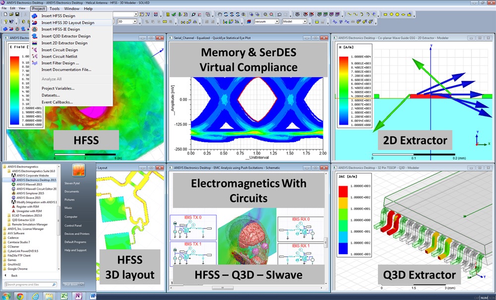
Yorgos replied, “Ansys HFSS is the gold standard for electromagnetic analysis, spanning the gamut from wireless propagation to PCB-level signal and power integrity simulation. The previous generation RaptorX product focused on parasitic calculations for on-chip structures – such as spirals, power grids, on-die MIM decoupling capacitors. We have merged HFSS and RaptorX into RaptorH. Both engines are integrated. Designers leverage the best of both algorithms automatically – the tool applies the optimum approach to each element of the model.”
Anand added, “Several considerations were an integral part of the RaptorH product development. A silicon-centric design environment is the basis for these 2.5D and 3D packages. GDS-II or OASIS data represents the design. The techfile stackup definition utilizes the process description from the foundry. All layer and dimensional information is encrypted. Process corner definitions use the same definitions as the traditional silicon environment.”
“Yorgos highlighted the focus on usability – how did that influence the product development?”, I inquired.
Anand replied, “The RaptorH desktop will be familiar to both current RaptorX and HFSS users. The 3D design geometry and the visualization of the electromagnetic field solution use the existing Ansys desktop interface.”

Anand continued, “Both S-parameter and circuit netlist models are provided. Of specific note is that this analysis is available pre-LVS, while designs are still in flight.”
I asked, “For general electromagnetic analysis, HFSS typically requires significant expertise at the controls – for example, the definition and placement of model ports. How is that managed in RaptorH?”
Anand replied, “The silicon-centric nature of the RaptorH flow means we needed to provide a familiar environment to chip designers. We don’t need to support free-space electromagnetics, waveguides, antennas, and the like. All metals are created equal. Designers set circuit ports just as if they were placing a probe tip in the lab.”
I asked, “These 2.5D and 3D package model databases can be huge – how is the RaptorH tool performance?”
Yorgos answered, “The intent of RaptorH is to present the entire layout for EM analysis. No pruning of data lanes required, hoping the sampled topology is representative of the full interface. The tool quickly analyzes the footprint of the design, the ports, and techfile stackup data to provide guidelines on the computational resources needed – that algorithmic analysis takes a small percentage of the total computation time. EM model generation is extremely parallelizable. For very large problems, RaptorH utilizes multiprocessing cloud resources, with an excellent speedup factor when using multiple processors.”
If you are pursuing a 2.5D/3D packaging solution, accurate signal and power distribution model extraction is an absolute necessity. I would encourage you to investigate the unique features of the Ansys RaptorH solution. Specifically, there is a brief webinar available discussing electromagnetic coupling within these complex systems, that provides lots of additional information – I learned a lot.
Ansys RaptorH Pre-LVS Electromagnetic Modeling — link.
Ansys RaptorH webinar: De-Risking High-Speed Serial Links from On-Chip Electromagnetic Crosstalk and Distribution Issues — link.
-chipguy
References
[1] Restle, P., et al., “Measurement and Modeling of On-Chip Transmission Line Effects in a 400MHz Microprocessor”, IEEE Journal of Solid State Circuits, Vol. 33, No. 4, April 1998, p 662-665.
Also Read
Need Electromagnetic Simulations for ICs?
Webinar: Electrothermal Signoff for 2.5D and 3D IC Systems
Best Practices are Much Better with Ansys Cloud and HFSS
Share this post via:


Comments
There are no comments yet.
You must register or log in to view/post comments.