







Electronic Design Automation, or EDA, is the software infrastructure that transforms a hardware specification into a manufacturable integrated circuit. At advanced process nodes, the problem is no longer simply drawing transistors or connecting gates. A modern system-on-chip contains billions of standard cells, hundreds of clock and power domains, dense SRAM macros, high-speed interfaces, embedded analog blocks, and often chiplet or advanced-package integration. EDA tools manage this complexity by converting register-transfer level descriptions into optimized physical layouts while proving that the resulting design satisfies functional, electrical, timing, and manufacturing constraints.
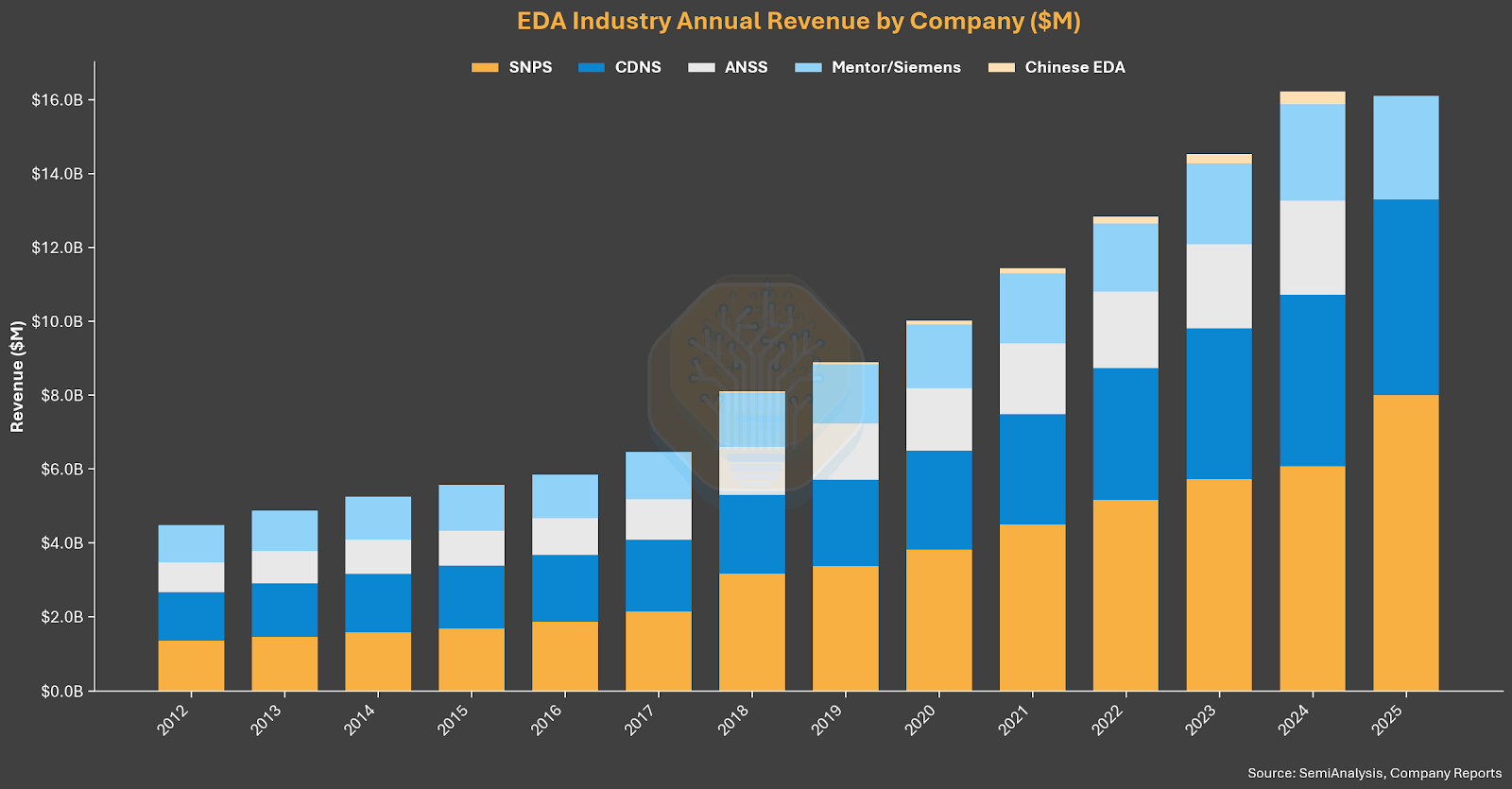
The flow begins with RTL written in Verilog, SystemVerilog, or VHDL. Logic synthesis maps this RTL into a gate-level netlist using a process-specific standard-cell library. The synthesis engine must optimize Boolean logic under timing, area, power, and testability constraints while respecting library characterization across process, voltage, and temperature corners. For high-performance designs, synthesis is not a single pass. Engineers iterate constraints, clock definitions, hierarchy boundaries, retiming options, and physical-awareness settings to reduce critical-path delay before physical implementation.
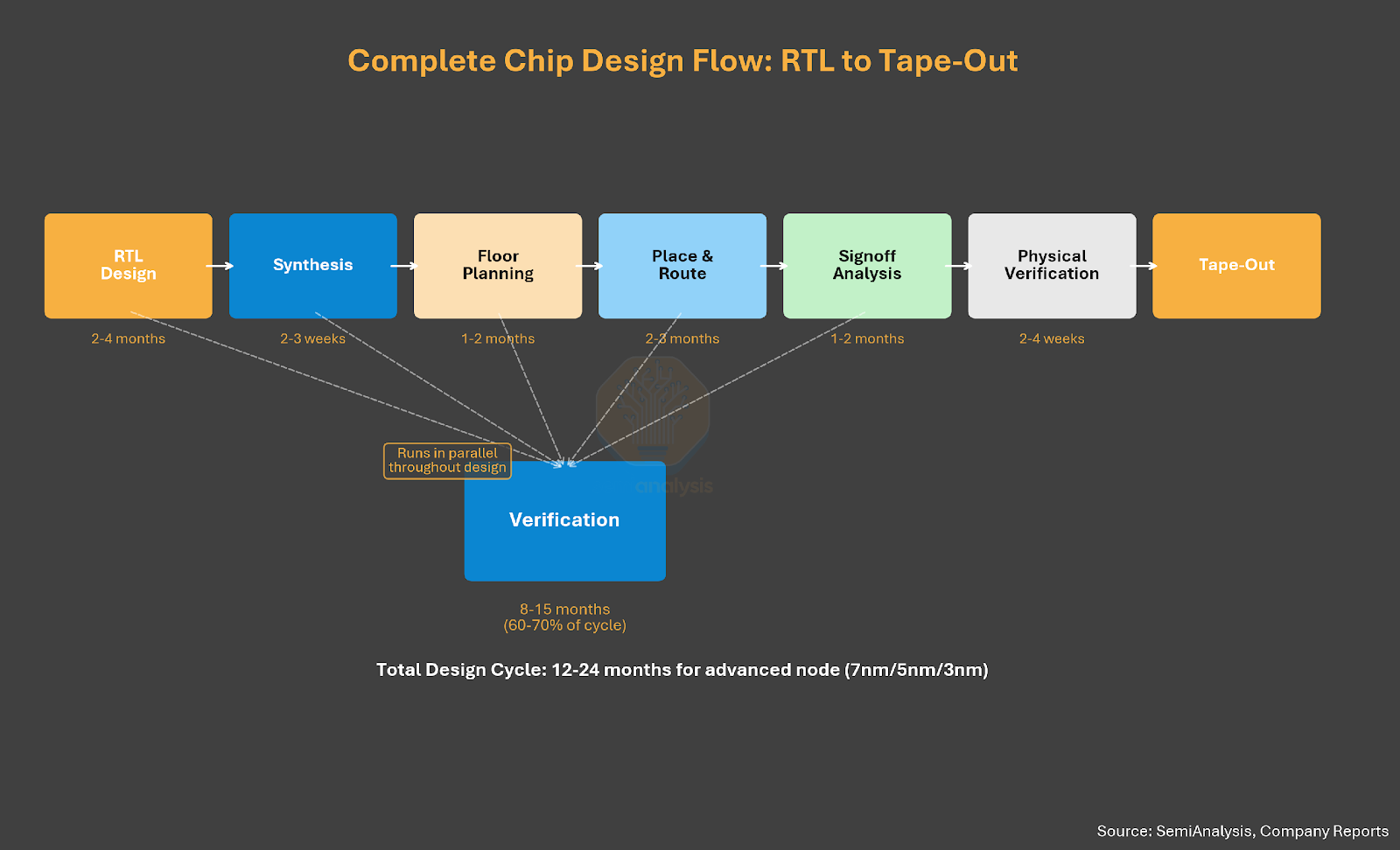
Physical design then converts the netlist into layout. Floorplanning defines macro placement, power grids, clock topology, voltage islands, and routing resources. Placement engines position millions or billions of instances while minimizing wirelength, congestion, timing violations, and power density. Clock-tree synthesis inserts buffers and balances skew across clock domains. Routing tools assign interconnect across many metal layers while obeying spacing, width, via, electromigration, multi-patterning, and density rules. At leading-edge nodes, routing is constrained by thousands of design rules, and local layout decisions can affect yield, timing, IR drop, and signal integrity simultaneously.
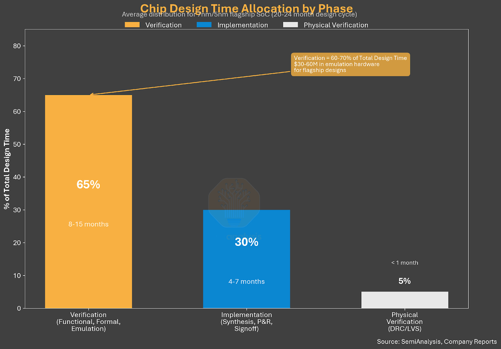
Signoff analysis verifies that the physical implementation is electrically robust. Static timing analysis checks setup and hold closure across many PVT scenarios, extracted parasitics, clock uncertainties, and on-chip variation models. Parasitic extraction calculates resistance, capacitance, and coupling effects from the final routed layout. Power integrity tools evaluate dynamic and static IR drop, electromigration, and local current density. Signal-integrity analysis checks crosstalk-induced delay shifts and noise. These analyses are interdependent: fixing timing can worsen congestion, reducing IR drop can increase area, and changing routing can alter parasitics enough to reopen timing violations.
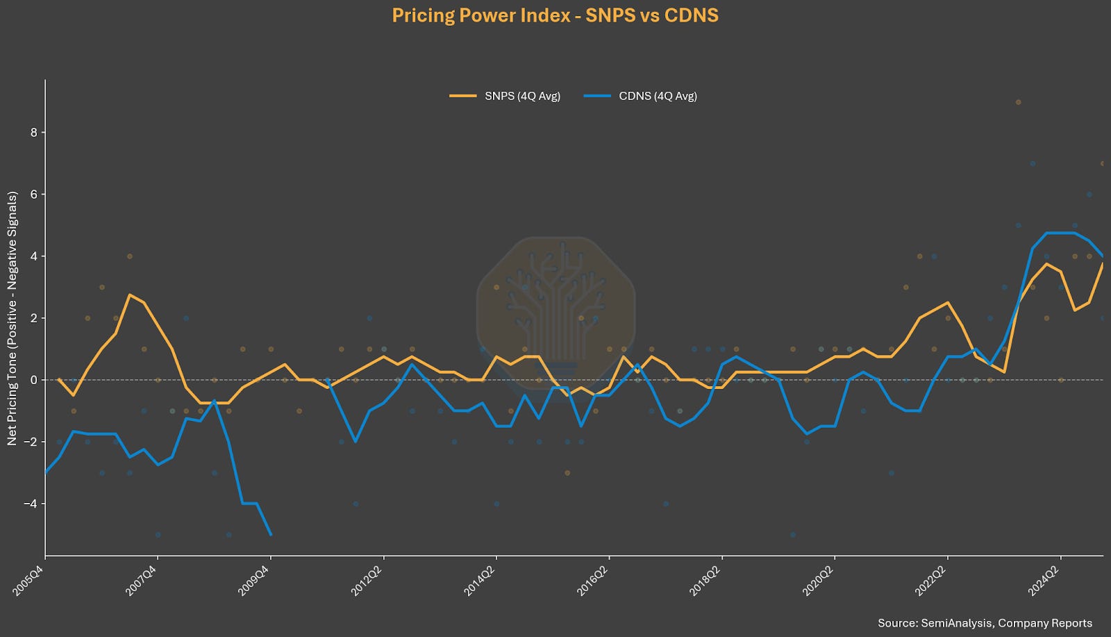
Functional verification is usually the largest engineering workload. Simulation runs directed and constrained-random tests against RTL and gate-level models. Formal verification proves equivalence between RTL and synthesized netlists, checks protocol properties, and validates unreachable-state assumptions. Coverage tools track exercised states, transitions, assertions, and functional scenarios. For large SoCs, hardware emulation maps the design onto specialized hardware so firmware, drivers, operating systems, and system workloads can run before silicon returns. This is essential for AI accelerators and datacenter processors, where full-stack validation requires interactions among compute arrays, memory controllers, interconnect fabrics, PCIe, CXL, HBM, security engines, and software runtime layers.
Physical verification is the final manufacturing gate. Design rule checking verifies compliance with foundry geometry constraints. Layout-versus-schematic comparison proves that the mask layout implements the intended circuit. Antenna checks, density checks, lithography-aware checks, and reliability checks reduce manufacturing and lifetime-failure risk. The final output is a GDSII or OASIS database delivered to the foundry for mask generation and wafer fabrication.
The engineering lock-in in EDA comes from flow dependency. Tool outputs are not isolated artifacts; each stage feeds constraints, models, reports, and databases into the next. A change in synthesis can alter placement. A placement change can affect routing. Routing changes modify parasitics. Parasitic changes can break timing, power integrity, or signal integrity. Because of this dependency graph, design teams build extensive internal scripts, regression systems, signoff checklists, and debug methodologies around specific toolchains.
Bottom line: The technical value of EDA is therefore not just automation. It is convergent optimization under extreme constraint density. The tools must search enormous design spaces while producing results that are functionally correct, timing-clean, power-compliant, manufacturable, and economically competitive. As process nodes shrink and systems move toward chiplets, advanced packaging, and AI-driven design-space exploration, EDA is becoming an integrated optimization platform spanning RTL, silicon, package, board, thermal, electromagnetic, and system-level verification.
Reference:
EDA Market Primer – Market Dynamics, Cadence, Synopsys, Siemens, China EDA Rise
Also Read:
See Autonomous Chip Design in Action with ChipAgents at DAC 2026
Demonstrating the EasyAI ECO Suite – An AI-Powered Functional ECO Solution at DAC 2026
Podcast EP353: What Real-Time Visibility Is and Why it Matters with yieldHUB’s John O’Donnell
Share this post via:



TSMC’s AI Expansion Signals a Broader Shift in Computing