FPGA Prototyping is growing in popularity as a method to get an SoC design into hardware running at clock speeds up to 100MHz or so. One downside during traditional FPGA prototyping debug is the limited number of internal signals that you can observe while trying to chase down bugs in the hardware design in the presence of running real software and drivers.
Research done by Brad Quinton as a PhD student at the University of British Columbia led directly to a startup called Veridae Systems in 2009 that addressed this issue of observing dramatically more internal signals of the FPGA prototype. Brad then sold Veridae Systems to the Embedded Instrumentation Group at Tektronix in July 2011.

I met with Brad Quinton at Tektronix in Beaverton last month to hear his story and better understand how this technology reduces the time it takes to debug an FPGA prototype.
Old Debug Approach
FPGA vendors have software (Xilinx Chipscope or Altera Signal tap) that let a designer choose a list of internal signals for debugging, and these signals are stored inside of RAM on the chip and later read out to debug. The problems associated with this approach are:
- You don’t know ahead of time which signals to start looking at, so you must iterate until you find useful internal signals.
- The number of signals that you can specify is limited.
- Every time that you choose a different set of internal signals you must re-compile the design, taking hours per iteration on large designs.
New Debug Approach
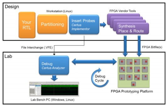
Tektronix has a new EDA tool called Certus2.0 that fits into any FPGA Prototyping tool flow:

Features that will save you time and effort in debugging are:
- Add all the FSM registers, all Flip-Flops, or any internal signal in a design for analysis.
- Low impact on using up FPGA resources.
- Eliminates the old synthesis recompile loop.
Bugs that used to take you literally days to identify and find now can take you just minutes. There are no more “Go Home Events” when you debug an FPGA prototype using Certus.
How Certus Works
The exact techniques are patented however in general the Certus approach changes your RTL description and uses hardware compression to minimize FPGA resource usage.
Q&A
Q: Would my FPGA timing change when using Certus?
A: Normally not, because Certus is just reading values of internal signals.
Q: Is there any limit in clock domains?
A: You can have up to 256 independent domains per FPGA.
Q: How long would I use Certus in a typical FPGA design project?
A: On a 1 year project from RTL to tapeout with another 1 year from tapeout to production, we recommend that you start prototyping when RTL is solid, and then use Certus for 6 months on a 2 year project.
Q: How is Certus licensed?
A: Certus uses floating licenses like most EDA tools.
Q: How much overhead is Certus adding to my design?
A: It varies, and could up to 10% to add this massive visibility.
Q: What HDL languages are supported?
A: We support VHDL, Verilog and SystemVerilog languages.
Q: How efficient is your compression efficiency?
A: In a single Block RAM we can typically store millions of trace depth.
Q: How is the debug output with Certus different from using FPGA Vendor tools?
A: With their tools you can only view a small number of internal signals per FPGA chip and per clock domain, while with Certus you see all the internal signals added across all FPGAs and clock domains simultaneously.
Q: Who would benefit from using Certus?
A: Firmware and software developers will definitely speed up their debug process, plus they won’t have to spend $1M+ on a an emulator because they can use Certus for just $25K to $75K.
Q: How long does it take an engineer to learn the Certus tool and flow?
A: We see engineers come up to speed within a day to learn Certus.
Summary
Debugging an FPGA prototype used to take weeks however with a new approach from Tektronix called Certus that debug time can be reduced to hours or days. This time reduction is enabled by giving the engineer a huge observation network, deep captures correlated across multiple chips, and no more long re-synthesis loops.
Further Reading
Share this post via:


Solving the EDA tool fragmentation crisis