You are currently viewing SemiWiki as a guest which gives you limited access to the site. To view blog comments and experience other SemiWiki features you must be a registered member. Registration is fast, simple, and absolutely free so please,
join our community today!
Near the end of any large SoC design project, the RTL code is nearly finished, floorplanning has been done, place and route has a first-pass, static timing has started, but the timing and power goals aren’t met. So, iteration loops continue on blocks and full-chip for weeks or even months. It could take a design team 5-7 days… Read More
Dan is joined by Brandon Bautz, Sr. Group Director of Product Management, responsible for the Cadence silicon signoff and verification product lines in the Digital & Signoff Group.
Dan and Brandon explore the substantial challenges faced by design teams needing to perform full-chip signoff at an accelerated pace for advanced… Read More
In the spectrum of functional verification platforms – software-based simulation, emulation and FPGA-based prototyping – it is generally agreed that while speed shoots up by orders of magnitude (going left to right) ease of debug drops as performance rises and setup time increases rapidly, from close to nothing for simulation… Read More
Steve Bailey entertained us during lunch on Tuesday with a talk on debug and visualization in the Mentor platform. Steve is based in Colorado, so had to spend the first part of his talk gloating about their Super Bowl win, but I guess he deserves that.
On a more technical note, he showed us a familiar survey they had completed with the… Read More
ASIC prototyping from multiple vendors using FPGA boards was popular at DAC again this year in Austin, Texas. I stopped by the Tektronix booth for a few minutes to meet with Dave Orecchio to get an update.
Dave Orecchio (right), Tektronix… Read More
As an engineer I learn new concepts best by seeing a demonstration, in this case it was a demo of how to optimize SoC performance by using an ASIC prototyping debug process. SoC designers that use FPGAs to prototype their new ASIC often encounter debug issues, like:
- Limited observability of internal nets required for debug, maybe
…
Read More
Tektronix at #50DACby Daniel Nenni on 05-13-2013 at 10:00 amCategories: EDA
If we grew up in similar eras you will know Tektronix as a company that manufactures test and measurement devices. Every lab I was in during high school and college had Tek oscilloscopes and logic analyzers. At #50DAC however, attendees that visit Tektronix will experience firsthand RTL simulation-level visibility to multi-FPGA… Read More
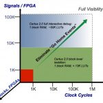
ASIC prototyping in FPGAs is starting to trend on SemiWiki. As FPGA technology becomes more advanced customers tell me that the traditional debug tools are inadequate. Faced with the very restrictive debugging capabilities and very long synthesis/place/route times the debugging cycle in these prototype platforms are quite… Read More
As RTL designs in FPGA-based ASIC prototypes get bigger and bigger, the visibility into what is happening inside the IP is dropping at a frightening rate. Where designers once had several hundred observation probes per million gates, those same several hundred probes – or fewer if deeper signal captures are needed – are now spread… Read More
FPGA Prototyping is growing in popularity as a method to get an SoC design into hardware running at clock speeds up to 100MHz or so. One downside during traditional FPGA prototyping debug is the limited number of internal signals that you can observe while trying to chase down bugs in the hardware design in the presence of running … Read More