As RTL designs in FPGA-based ASIC prototypes get bigger and bigger, the visibility into what is happening inside the IP is dropping at a frightening rate. Where designers once had several hundred observation probes per million gates, those same several hundred probes – or fewer if deeper signal captures are needed – are now spread across 10M gates or more.
That sparseness causes choices, and if through divine inspiration probes are placed where the problem is, there is some debug visibility to help solve issues. Most engineers aren’t that fortunate, especially with unfamiliar third party IP, and debugging is trial-and-more-error. While probes can be moved around in an FPGA-based prototype until the problem is isolated, re-synthesis is a process that takes hours, usually reserved for overnight runs.
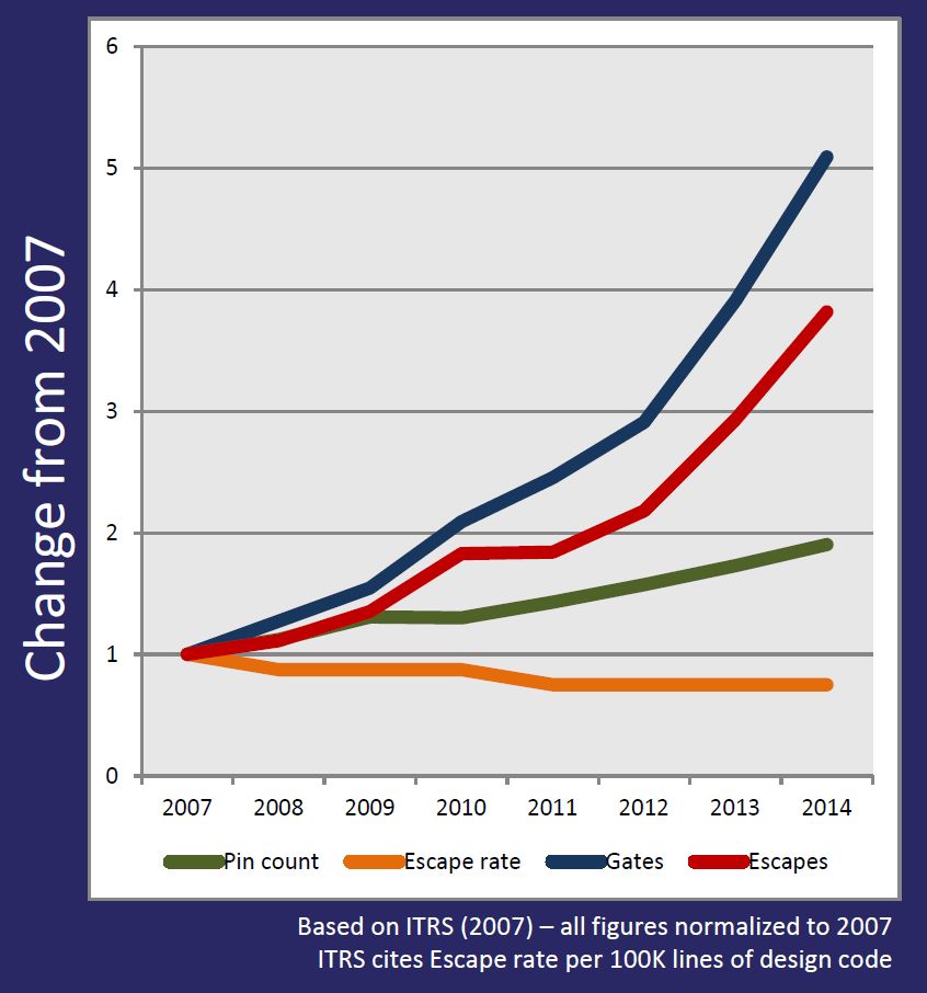
Daniel Payne gives us an introduction to Brad Quinton, creator of the technology inside the Tektronix Certus 2.0 FPGA-based prototyping debug solution. I’d first heard about Brad’s approach in 2010, prior to his company Veridae Systems being acquired by Tektronix. He used the following chart from ITRS to illustrate the problem:

While the escape rate of bugs per 100K lines of code (LOCs) improves, it is outstripped by the growth in RTL LOCs for bigger designs, and the result is an out-of-control increase in escapes. The issue Brad has been after is how to add more probes to an RTL design without chewing up major resources in an FPGA.
There are several key technologies in play in Certus:
Efficient embedded instrumentation: A small block of RTL comprising a probe can be placed on just about anything in the FPGA, connected to an infrastructure with a multi-stage concentrator using fewer LUTs than traditional probes in FPGAs. These placements are done automatically using the Implementor tool in any FPGA EDA flow, and it allows control over how many LUTs are allocated to the debug infrastructure. Using OptiRank, design RTL is analyzed, and signals are ranked producing recommendations for the best coverage.

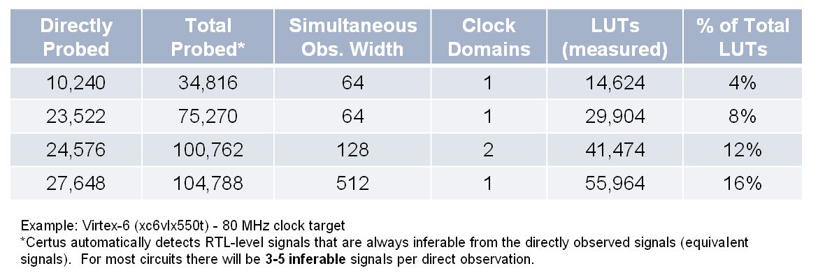
Longer debug traces: Traditional FPGA probing can capture limited amounts of data, usually a few seconds, at-speed. However, to see problems develop, often more than a few seconds of data is needed, a difficult task for on-chip resources with limited RAM. External analyzers can be used but they have to be synchronized carefully. In Certus, capture data from each probe is compressed in a lossless algorithm which takes advantage of repeated patterns common in traces, resulting in extended trace depths. These figures aren’t typical but represent what is possible in trace depths:

Time-correlation analysis:Certus collects time-correlated data system wide from all the probes at full speed of the FPGA-prototyping system, and presents it on a single JTAG interface. Using the Analyzer tool, designers can zoom in and create complex triggers on the data of interest. Instead of re-instrumenting and re-synthesizing the FPGA, designers can just run scenarios and go to the data. Another benefit of this is unique to FPGA-based prototyping systems: since the data collected from multiple FPGAs is time-correlated, partitioning problems and issues with multiple clock domains can be identified quickly and easily.
In significantly less time than it would take a designer to place 1K probes using traditional tools, up to 100K probes can be placed using Certus. Once that placement is synthesized in, designers can concentrate on running scenarios and analyzing and fixing design RTL instead of recompiling instrumentation just to identify the issues.
The Tektronix approach in Certus brings instrumentation to any FPGA-based prototyping system, creating the opportunity for much deeper visibility similar to an RTL simulator or emulator, but with much faster speeds of operation. See the Tektronix White Papers Wiki for a white paper describing bottlenecks Certus addresses, and a case study from the Dini Group on Certus use.
Share this post via:


Is Intel About to Take Flight?