You are currently viewing SemiWiki as a guest which gives you limited access to the site. To view blog comments and experience other SemiWiki features you must be a registered member. Registration is fast, simple, and absolutely free so please,
join our community today!
            WP_Term Object
(
    [term_id] => 1561
    [name] => ESD Alliance
    [slug] => esd-alliance
    [term_group] => 0
    [term_taxonomy_id] => 1561
    [taxonomy] => category
    [description] =>
    [parent] => 386
    [count] => 120
    [filter] => raw
    [cat_ID] => 1561
    [category_count] => 120
    [category_description] =>
    [cat_name] => ESD Alliance
    [category_nicename] => esd-alliance
    [category_parent] => 386
    [is_post] =>
)

WP_Term Object
(
    [term_id] => 1561
    [name] => ESD Alliance
    [slug] => esd-alliance
    [term_group] => 0
    [term_taxonomy_id] => 1561
    [taxonomy] => category
    [description] =>
    [parent] => 386
    [count] => 120
    [filter] => raw
    [cat_ID] => 1561
    [category_count] => 120
    [category_description] =>
    [cat_name] => ESD Alliance
    [category_nicename] => esd-alliance
    [category_parent] => 386
    [is_post] =>
)
At Semicon I met with Applied Materials to learn about epitaxy. This is when a monocrystalline film is grown on the substrate which takes on a lattice structure that matches the substrate. It forms a high purity starting point for building a transistor and is also the basis of the strain engineering in a modern process.
Since holes… Read More
Round #1 was here.
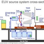
In the EUV corner were Stefan Wurm of Sematech (working on mask issues mostly) and Skip Miller of ASML who are the only company making EUV steppers (and light sources, they acquired Cymer).
You may know that the biggest issue in EUV is getting the source brightness to have high enough energy that an EUV stepper has … Read More
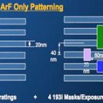
If you want to know the state of play in lithography, there is no better place than the special session on lithography at Semicon West. This year was no exception. The session was given the punchy title Still a tale of 2 paths: multi-patterning lithography at 20nm and below: EUVL source and infrastructure progress.
In the blue corner… Read More
My friend and fellow blogger Kurt Shuler wrote recently, “DAC Is Dead? Long Live DAC!”, which is worth a click over. In addition to providing a nice attendance graph and the top three reasons why it is NOT all rosy, Kurt suggests colocating DAC with other conferences (DESIGN West) but fails to mention SEMICON West.
SEMICON West is … Read More
SEMICON West is next week, July 9-11 in San Francisco. If you haven’t signed up, and want to attend for free instead of $100,
1) Send an email to silicon_test@mentor.com with subject line “Semicon pass.”
2) Register for SEMICON West
3) After registering, download the SEMICON West mobile app and start building your schedule. Here… Read More
I will be at Semicon West from 9th to 11th July in Moscone, San Francisco. Of course there are lots of interesting sessions but here are two that I think are especially important to get a good impression of the way things are going in the future from experts. The two most interesting questions about the future are what comes after 14nm,… Read More
They are three of the top trending terms on SemiWiki and three of the hot topics at this year’s Semicon West:
In its 43rd year, SEMICON West is the flagship annual event for the global microelectronics industry. It is the premier event for the display of new products and technologies for microelectronics design and manufacturing,… Read More
So where in the world do you think semiconductor manufacturing is increasing the fastest? OK, Taiwan, that was pretty easy. But in second place, with over 20% of the world’s semiconductor equipment capital investment is the US. Growing faster than Europe, China, Japan and equal with Korea.
This was not the case half a dozen… Read More
I’ve been digging around the Interwebs a bit trying to find out what the received wisdom is about how big a cost reduction can be expected if and when we transition to 450mm (18″) wafers from today’s standard of 300mm (12″). And the answers are totally all over the place. They vary from about a 30% cost reduction… Read More
At Semicon, Ben Rathsack of Tokyo Electron America talked about directed self assembly (DSA) at the standing-room only lithography morning. So what is it? Self assembly involves taking two monomers that don’t mix and letting them polymerise (so like styrene forming polystyrene). Since they won’t mix they will … Read More