You are currently viewing SemiWiki as a guest which gives you limited access to the site. To view blog comments and experience other SemiWiki features you must be a registered member. Registration is fast, simple, and absolutely free so please,
join our community today!
WP_Term Object
(
    [term_id] => 16126
    [name] => Lithography
    [slug] => lithography
    [term_group] => 0
    [term_taxonomy_id] => 16126
    [taxonomy] => category
    [description] =>
    [parent] => 0
    [count] => 190
    [filter] => raw
    [cat_ID] => 16126
    [category_count] => 190
    [category_description] =>
    [cat_name] => Lithography
    [category_nicename] => lithography
    [category_parent] => 0
    [is_post] =>
)
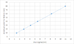
Lithography has been the driving force for shrinking feature sizes for decades, and the most easily identified factor behind this trend is the reduction of wavelength. G-line (436 nm wavelength) was used for 0.5 um in the late 1980s [1], and I-line (365 nm wavelength) was used down to 0.3 um in the 1990s [2]. Then began the era of deep-ultraviolet… Read More
High-NA EUV has received a lot of attention ever since Intel put the spotlight on its receiving the first 0.55 NA EUV tool from ASML [1], expected in 2025. EUV itself has numerous issues which have been enumerated by myself and others, most notoriously the stochastic defects issue. There are also a host of issues related to the propagation… Read More
Recent advances in EUV lithography have largely focused on “low-k1” imaging, i.e., features with pitches less than the wavelength divided by the numerical aperture (k1<0.5). With a nominal wavelength of 13.5 nm and a numerical aperture of 0.33, this means sub-40 nm pitches. It is naturally expected that larger… Read More
– Strong demand across logic/memory & leading/trailing edge
– Customers want units fast-no time to test
– The main question is can ASML ramp to meet demand?
Revenue & Earnings low due to systems being rushed to customers
ASML reported Euro 4B in sales and Euro 1B in net income which while within guidance… Read More
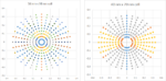
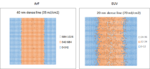
Due to the higher energy of EUV (13.3-13.7 nm wavelength) compared to ArF (193 nm wavelength) light, images produced by EUV are more susceptible to photon shot noise.
Figure 1. (Left) 40 nm dense (half-pitch) line image projected onto wafer at 35 mJ/cm2; (Right) 20 nm dense (half-pitch) line image projected onto wafer at 70 mJ/cm2.… Read More
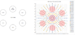
The stochastic behavior of images formed in EUV lithography has already been highlighted by a number of authors [1-3]. How serious it appears depends on the pixel size with which the photons are bunched. Generally, though, for features of around 20 nm or less, even 1 nm can have at least a +/- 15% gradient across it, which is still a
…
Read More
– KLA put up an excellent quarter and Guide
– Rising above the increasing tide of orders
– Confirms $75B capex in 2021 with upside
– Foundry & Logic continue to be the sweet spot for KLA
Business is very very good and getting better
-Revenues came in at $1.8B with EPS of $3.85, all above the range
-Guidance… Read More
In this article, we will explore the use of self-aligned litho-etch-litho-etch (SALELE) double patterning for BEOL metal layers in the 7nm node (40 nm minimum metal pitch [1]) with DUV, and 5nm node (28 nm minimum metal pitch [2]) with EUV. First, we mention the evidence that this technique is being used; Xilinx [3] disclosed the… Read More
At the SPIE Advanced Lithography Conference held in February, ASML presented the latest information on their Deep Ultraviolet (DUV) and Extreme Ultraviolet (EUV) exposure systems. I recently got to interview Mike Lercel of ASML to discuss the presentations.
DUV
Despite all the attention EUV is getting, most layers are still… Read More
I recently posted an insightful article [1] published in 2013 on the cost of 3D NAND Flash by Dr. Andrew Walker, which has since received over 10,000 views on LinkedIn. The highlight was the plot of cost vs. the number of layers showing a minimum cost for some layer number, dependent on the etch sidewall angle. In this article, the same… Read More


TSMC CoWoS versus Intel EMIB Semiconductor Packaging