You are currently viewing SemiWiki as a guest which gives you limited access to the site. To view blog comments and experience other SemiWiki features you must be a registered member. Registration is fast, simple, and absolutely free so please,
join our community today!
WP_Term Object
(
    [term_id] => 16126
    [name] => Lithography
    [slug] => lithography
    [term_group] => 0
    [term_taxonomy_id] => 16126
    [taxonomy] => category
    [description] =>
    [parent] => 0
    [count] => 190
    [filter] => raw
    [cat_ID] => 16126
    [category_count] => 190
    [category_description] =>
    [cat_name] => Lithography
    [category_nicename] => lithography
    [category_parent] => 0
    [is_post] =>
)
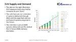
In my “The EUV Divide and Intel Foundry Services” article available here, I discussed the looming EUV shortage. Two days ago, Intel announced their first EUV tool installed at their new Fab 34 in Ireland is a tool they moved from Oregon. This is another indication of the scarcity of EUV tools.
I have been tracking EUV system production… Read More
At the ISS conference held from April 4th through 6th I presented on who I thought would have the leading logic technology in 2025. The following is a write up of that presentation.
ISS was a virtual conference in 2021 and I presented on who currently had logic leadership and declared TSMC the clear leader. Following that conference,… Read More
Stochastic defects continue to draw attention in the area of EUV lithography. It is now widely recognized that stochastic issues not only come from photon shot noise due to low (absorbed) EUV photon density, but also the resist material and process factors [1-4].
It stands to reason that resist absorption of EUV light, which is … Read More
The 5nm foundry node saw the arrival of 6-track standard cells with four narrow routing tracks between wide power/ground rails (Figure 1a), with minimum pitches of around 30 nm [1]. The routing tracks require cuts [2] with widths comparable to the minimum half-pitch, to enable the via connections to the next metal layer with the… Read More
The EUV Divide
I was recently updating an analysis I did last year that looked at EUV system supply and demand, while doing this I started thinking about Intel and their Fab portfolio.
If you look at Intel’s history as a microprocessor manufacturer, they are typically ramping up their newest process node (n), in volume production… Read More
EUV lithography systems continue to be the source of much hope for continuing the pace of increasing device density on wafers per Moore’s Law. Recently, although EUV systems were originally supposed to help the industry avoid much multipatterning, it has not turned out to be the case [1,2]. The main surprise has been the
…
Read More
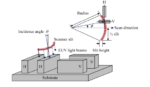
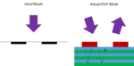
As EUV lithography is being targeted towards pitches of 30 nm or less, fundamental differences from conventional DUV lithography become more and more obvious. A big difference is in the mask use. Unlike other photolithography masks, EUV masks are absorber patterns on a reflective multilayer rather than a transparent substrate.… Read More
In previous articles, I had looked at EUV stochastic behavior [1-2], primarily in terms of the low photon density resulting in shot noise, described by the Poisson distribution [3]. The role of blur to help combat the randomness of EUV photon absorption and secondary electron generation and migration was also recently considered… Read More
Lithography is arguably the most important step in semiconductor manufacturing. Today’s state-of-the-art EUV scanners are incredibly complex machines that cost as much as a new Boeing jetliner.
From humble beginnings in 1984 as a joint venture with Philips, ASML has grown to become the world’s second largest chip equipment… Read More
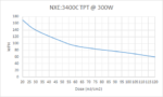
Recently, a patent application from TSMC [1] revealed target EUV doses used in the range of 30-45 mJ/cm2. However, it was also acknowledged in the same application that such doses were too low to prevent defects and roughness. Recent studies [2,3] have shown that by considering photon density along with blur, the associated shot… Read More


TSMC CoWoS versus Intel EMIB Semiconductor Packaging