You are currently viewing SemiWiki as a guest which gives you limited access to the site. To view blog comments and experience other SemiWiki features you must be a registered member. Registration is fast, simple, and absolutely free so please,
join our community today!
WP_Term Object
(
    [term_id] => 89
    [name] => FinFET
    [slug] => finfet
    [term_group] => 0
    [term_taxonomy_id] => 89
    [taxonomy] => category
    [description] =>
    [parent] => 0
    [count] => 232
    [filter] => raw
    [cat_ID] => 89
    [category_count] => 232
    [category_description] =>
    [cat_name] => FinFET
    [category_nicename] => finfet
    [category_parent] => 0
    [is_post] =>
)
Summary
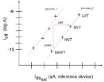
As a result of extensive focus on the development of workfunction metal (WFM) deposition, lithography, and removal, both FinFET and gate-all-around (GAA) devices will offer a wide range of Vt levels for advanced process nodes below 7nm.
Introduction
Cell library and IP designers rely on the availability of nFET and pFET… Read More
Summary
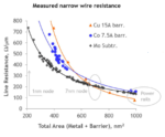
Design Technology Co-Optimization (DTCO) analysis was pursued for library cell PPA estimates for gate-all-around (GAA) devices and new metallurgy options. The cell design and process recommendations are a bit surprising.
Introduction
During the “golden years” of silicon technology evolution that applied Dennard… Read More
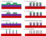
Self-aligned quadruple patterning (SAQP) is the most widely available technology used for patterning feature pitches less than 38 nm, with a projected capability to reach 19 nm pitch. It is actually an integration of multiple process steps, already being used to pattern the fins of FinFETs [1] and 1X DRAM [2]. These steps, shown… Read More
Talking Sense With Moortec…Are You Listening?!by Tim Penhale-Jones on 05-04-2020 at 10:00 amCategories: FinFET, IP, Moortec
It almost doesn’t matter what your job may be, whether in the public sector or a private company, or how technical or how dangerous, many of life’s adages and sayings can be interpreted to have some direct meaning for all of us.
Over the years in our personal lives, we have been constantly advised that prevention is better than cure…certainly… Read More
We live in an age of abundant information. There is a tremendous exchange of ideas crisscrossing the world enabling new innovative type of products to pop up daily. Therefore, in this era there is a greater need to understand competitive intelligence. Corporate companies today are interested in what other competitors are brewing… Read More
Our friends at Threshold Systems have a new class that may be of interest to you. It’s an updated version of the Advanced CMOS Technology class held last May. As part of the previous class we did a five part series on The Evolution of the Extension Implant which you can see on the Threshold Systems SemiWiki landing page HERE. And… Read More
Advanced IC technologies, 5nm and 7nm FinFET design and stacked packaging, are enabling massive levels of integration of super-fast circuits. These in turn enable much of the exciting new technology we hear so much about: mobile gaming and ultra-high definition mobile video through enhanced mobile broadband in 5G, which requires… Read More
IEDM is in my opinion the premiere conference for information on state-of-the-art semiconductor processes. In “My Top Three Reasons to Attend IEDM 2019” article I singled out the TSMC 5nm paper as a key reason to attend.
IEDM is one of the best organized conferences I attend and as soon as you pick up your badge you are handed a memory… Read More
The International Electron Devices Meeting is a premier event to learn about the latest in semiconductor process technology. Held every year in early December is San Francisco this years conference will be held from Decembers 7th through December 11th. You can learn more about the conference at their web site here.
This is a must… Read More
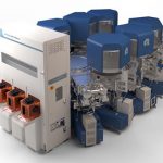
Tuesday July 9th was the first day the show floor was open at Semicon. The following is a summary of some announcements I attended and general observations.
AMAT Announcement
My day started with an Applied Materials (AMAT) briefing for press and analysts where they announced “the most sophisticated system they have ever released”.… Read More


Intel: Pushing EMIB Forward: Design Methodology Insights with Synopsys Tools