You are currently viewing SemiWiki as a guest which gives you limited access to the site. To view blog comments and experience other SemiWiki features you must be a registered member. Registration is fast, simple, and absolutely free so please,
join our community today!
WP_Term Object
(
    [term_id] => 89
    [name] => FinFET
    [slug] => finfet
    [term_group] => 0
    [term_taxonomy_id] => 89
    [taxonomy] => category
    [description] =>
    [parent] => 0
    [count] => 233
    [filter] => raw
    [cat_ID] => 89
    [category_count] => 233
    [category_description] =>
    [cat_name] => FinFET
    [category_nicename] => finfet
    [category_parent] => 0
    [is_post] =>
)
The industry recently concluded a series of technology events for the all the major foundries. Done as virtual events this year, each one provided a significant update on technology platforms, roadmaps and ecosystem partnerships. These events are quite valuable to chip design teams who need to be aware of the latest in process,… Read More
Seeking Alpha just published an article about Intel and Samsung passing TSMC for process leadership. The Intel part seems to be a theme with them, they have talked in the past about how Intel does bigger density improvements with each generation than the foundries but forget that the foundries are doing 5 nodes in the time it takes… Read More
SoC designs are getting more complex, resulting in a higher level of difficulty to get anything done. This trend is well-known. What I want to focus on here is how to deal with the issue of complexity. There are many approaches to taming this problem — faster algorithms for one, and improved algorithm efficiency or the ability to run… Read More
With the announcement of early PDK availability for the 3nm GAA process node, designers are extremely interested in the characteristics of the new “gate-all-around” transistor structure and how it compares to the existing FinFET device. The GAA transistor has been denoted as a (horizontal) nanowire or nanosheet.
I will talk… Read More
TSMC is the bellwether for not just the semiconductor industry but the worldwide economy. TSMC makes semiconductors, semiconductors are where electronics begin and electronics are the foundation of modern life, absolutely.
Apple is also a key economic indicator and as we all know Apple is a strategic partner of TSMC. The Apple… Read More
From Moore’s Law to Moortec’s Law!by Tim Penhale-Jones on 09-20-2020 at 10:00 amCategories: FinFET, IP, Moortec
No-one likes being put on the spot and yet we all like a forecast…and as we all know, the only guarantee with a forecast is that it is wrong. Sports commentators have carved out a special niche for themselves with the ‘commentators curse’, just as they extol the virtues of an individual or a team, the sporting gods prove them wrong in … Read More
On Thursday July 9 Imec held a virtual technology forum. Imec is one of the premier research organizations working on semiconductor technology and their forums are always interesting. My area of interest is process technology and the following are my observation in that area from the forum.
Luc Van Den Hove
Luc Van Den Hove is the… Read More
I had the pleasure of spending time with Hiren Majmudar in preparation for the upcoming AI Accelerators webinar. As far as webinars go this will be one of the better ones we have done. Hiren has deep experience in both semiconductors and EDA during his lengthy career at Intel and now with a pure play foundry. He is intelligent, personable,… Read More
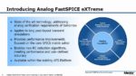
When Analog FastSPICE was first introduced in 2006 it changed the landscape for high performance SPICE simulation. During the last 14 years it has been used widely to verify advanced nanometer designs. Of course, since then the most advanced designs have progressed significantly, making verification even more difficult. Just… Read More
In this, the second part of a two-part series we delve further into defining worst case, this time focusing specifically on device performance.
In the last blog we talked about the steady increase in power density per unit silicon area and how worst case is definitely getting worse. We discussed how in each new FinFET node the dynamic… Read More

TSMC CoWoS versus Intel EMIB Semiconductor Packaging