You are currently viewing SemiWiki as a guest which gives you limited access to the site. To view blog comments and experience other SemiWiki features you must be a registered member. Registration is fast, simple, and absolutely free so please,
join our community today!
WP_Term Object
(
    [term_id] => 157
    [name] => EDA
    [slug] => eda
    [term_group] => 0
    [term_taxonomy_id] => 157
    [taxonomy] => category
    [description] => Electronic Design Automation
    [parent] => 0
    [count] => 4486
    [filter] => raw
    [cat_ID] => 157
    [category_count] => 4486
    [category_description] => Electronic Design Automation
    [cat_name] => EDA
    [category_nicename] => eda
    [category_parent] => 0
    [is_post] =>
)
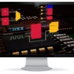
I live in Tualatin, Oregon just a few miles away from the corporate headquarters of the #3 EDA company in the world, Mentor Graphics. Since DAC is fast approaching, I thought it would be useful to give you a quick overview of what Mentor is going to be talking about in Austin, Texas during June 5-9. … Read More
When I hear the company name of ANSYS the first EDA tool category that comes to mind is power noise sign-off. Going to DAC is a great way to find out what’s new with EDA, IP and foundries. There are three places that you can find ANSYS at DAC this year:… Read More
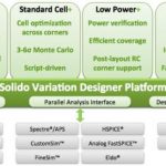
The design community is always hungry for high-performance, low-power, and low-cost devices. There is emergence of FinFET and FDSOI technologies at ultra-low process nodes to provide high-performance and low-power requirements at lower die-size. However, these advanced process nodes are prone to new sources of variation.… Read More
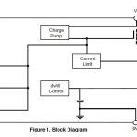
Power protection chips are widely used these days to protect sensitive circuitry from over-voltage and over-current stress. However, these workhorse chips are often subjected to extraordinary thermal stress themselves and need to be protected from burning up – literally.
Power protection chips work like electronic fuses,… Read More
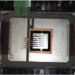
In the pages of SemiWiki, we are usually talking about what to do with billions of really small transistors – for a change of pace today, we’ll discuss what to do with a few really big ones. Mentor Graphics has just announced their latest MicReD platform for thermal testing of IGBTs, experiencing a resurgence (pun intended) thanks… Read More
Design starts are critical to the growth of the semiconductor industry so enabling them is a common theme on SemiWiki. One thing we have not covered in detail is multi-project wafer services (MPW) which is the equivalent of ride sharing through the initial mask and wafer process. Larger semiconductor companies already do this … Read More
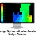
A common SoC design methodology in current use starts with preparation of the physical floorplan — e.g., block/pin placement, global clock domain and bus signal planning, developing the global/local power distribution (and dynamic power domain management techniques). Decoupling capacitor estimated densities and… Read More
Rebooting EDAby Bernard Murphy on 05-23-2016 at 7:00 amCategories: Ansys, Inc., EDA
In the 35 years since commercial EDA went mainstream a lot of advances have been made but the fundamental architecture and even the philosophy of tooling have really not advanced at all. Tools are designed around individual tasks – analysis and optimization within a specific domain – under the assumption that variability within… Read More
Markets work when consumers of a widget don’t feel there is significant differentiated value in making their own and would rather get lowest possible cost from experienced widget makers who can amortize their investment over high-volume sales to many customers. But that changes when a large consumer finds they can increase differentiated… Read More
This week I attended the UpWest Labs event in San Francisco. UpWest Labs provides seed funding and incubation for a wide range of domains including Enterprise Software, Internet of Things, Infrastructure Technologies, Artificial Intelligence, Consumer Applications, Drones, Cyber Security, Augmented Reality / Virtual … Read More


Intel: Pushing EMIB Forward: Design Methodology Insights with Synopsys Tools