Daniel is joined by Dr. Debendra Das Sharma, a Senior Fellow and Chief I/O architect in the Data Platforms and Artificial Intelligence Group at Intel. He is a member of the National Academy of Engineering (NAE), Fellow of IEEE, and Fellow of International Academy of AI Sciences. He is a leading expert on I/O subsystem and interface… Read More
The Chiplet Summit recently concluded. Multi-die heterogeneous design is a hot topic these days and chiplets are a key enabler for this trend. The conference was noticeably larger this year. There were many presentations and exhibits that focused on areas such as how to design chiplets, what standards are important, how to integrate… Read More
By Vikash Kumar, Senior Verification Architect | Arm | IEEE Senior Member.
The Problem Every Verification Engineer Recognizes
You ask an LLM to generate a UVM testbench. It produces 25 files. Everything compiles. You run the simulation — and nothing happens. The scoreboard reports zero checks. The slave driver stops after 10… Read More
In the rapidly evolving landscape of semiconductor technology, the Universal Chiplet Interconnect Express (UCIe) emerges as a groundbreaking open standard designed to revolutionize on-package chiplet integrations. Presented by Dr. Debendra Das Sharma, Chair of the UCIe Consortium and Intel Senior Fellow, at the Chiplet… Read More
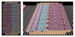
The semiconductor industry is entering a new era in system design. As traditional monolithic scaling approaches its economic and physical limits, multi-die architectures are emerging as a primary pathway for delivering continued improvements in performance, power efficiency, and integration density. By distributing … Read More
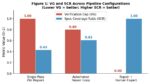
The first article in this series examined how feasibility exploration enables architects to evaluate multi-die system configurations while minimizing early design risk. Once architectural decisions are validated, designers must translate conceptual connectivity requirements into physical interconnect infrastructure.… Read More
At the 2026 Chiplet Summit, Synopsys presented a bold vision for the future of semiconductor innovation: AI-driven multi-die design powered by agentic intelligence. As the semiconductor industry shifts rapidly toward chiplet-based architectures and 3D stacking, the complexity of design, verification, and system integration… Read More
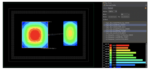
As analog and mixed-signal designs become increasingly complex, parasitic effects dominate both design time and cost, consuming 30–50% of engineers’ effort in debugging and reanalyzing circuits. Addressing these multiphysics effects requires early verification strategies and reliable simulation solutions. Modern … Read More
The rapid evolution of semiconductor design has elevated chiplets from a niche concept to a foundational strategy for next-generation computing. At the upcoming Chiplet Summit – February 17–19, 2026 Santa Clara Convention Center. Silicon Catalyst will play a central role in shaping this conversation, highlighting… Read More
The Design Automation Chips to Systems Conference is the preeminent international event for professionals involved in electronic design, system architecture, and EDA. Formerly known simply as the Design Automation Conference or DAC has evolved over more than six decades into a forward-looking forum that spans the entire… Read More


The Packaging PDK Is the Missing Layer for Co-Packaged Optics