




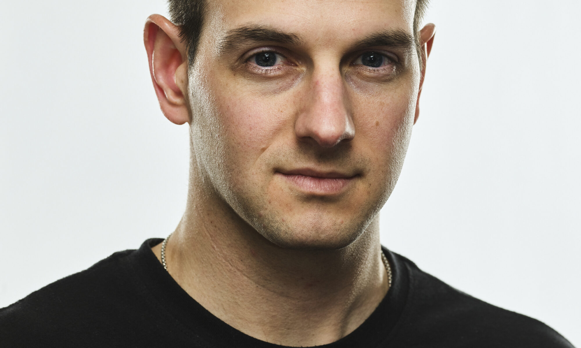




Joseph F. Krause is an American materials scientist, entrepreneur, and U.S. Army National Guard veteran. He is the cofounder and CEO of Radical AI, a New York deep-tech startup founded to accelerate the discovery of advanced materials.
Before Radical AI, Krause conducted nanomaterials research at Rice University, worked on neuromorphic semiconductors at the U.S. Army DEVCOM research laboratory, and led deep-tech investments at New York venture studio AlleyCorp.
He was selected for the 2026 Forbes 30 Under 30 list. Radical AI has also received a roughly $1.2 million U.S. Air Force contract to develop alloys for hypersonic applications. Some widely reported funding totals differ by date and source.
Tell us about your company?
Radical AI is building a new R&D process for materials. Today it can take decades and hundreds of millions of dollars to take an idea from lab to fab to a final semiconductor product. That slow pace of materials discovery limits semiconductor technology as a whole. And virtually every other future-facing industry—think space, nuclear fusion, advanced manufacturing—is held back by similar challenges.
We built a self-driving lab powered by AI. A human materials scientist inputs performance goals, then AI runs the entire interconnected research process: literature review, hypothesis generation, synthesis, characterization, physical testing in a real lab, total data capture, and active learning. The experimental findings feed back into this system to direct the next set of hypotheses. The process continues until it meets its material property and performance targets.
The company was founded in early 2024. We’re 42 people. We’ve raised $65 million and we have System One running right now in New York. We’re moving into a 45,000 square foot facility at the Brooklyn Navy Yard this fall to scale our capabilities.
What problems are you solving?
The core problem is that the scientific process for materials discovery is serial and slow. As a scientist (I was one before starting Radical) you walk the scientific method one step at a time. You read. You model. You hypothesize. You synthesize. You characterize, and you analyze. Weeks pass. Then you do it again. AI is extraordinary at doing that simultaneously and integrating feedback to judge what the next step should be. It can analyze SEM images while also reading 100,000 publications. That integration between idea, fabrication, characterization, and the next design of experiments is what changes everything.
For semiconductors, this hits where the industry struggles. Every major node transition, every new packaging architecture, every thermal challenge at the bleeding-edge node entails fundamental materials problems. We reduce the time it takes to go from an idea to a validated material down to weeks, not decades. It’s really significant that we focus on physical validation, instead of just modeling. A model without a physical execution layer misses what actually changes the world: the material and its interaction with the world around it. To be fair, delivering a final semiconductor chip has many other supply, defect, and yield challenges, but by starting out with a data-driven self-driving lab, the data is captured at every step along the way to inform the next stages of semiconductor materials integration.
What application areas are your strongest?
Our first system focuses on structural high entropy alloy metals for hypersonic applications. We’ve made over 1,000 novel compositions. A few of those showed 100x performance improvement over the existing industry-leading alloy. We’ve already moved onto the next step and sent the most promising materials to the Purdue Applied Research Institute to verify these findings.
In semiconductors, there are near-term opportunities we can already address in interconnects, dielectrics, and packaging materials. Interconnects are one of the most pressing challenges. As technology node scaling shrinks linewidths down to the nanometer level, the copper atoms “feel” the interface just a few nanometers away. The 5 nm thin film resistivity grows more than 10X vs. its bulk value. This is fundamentally a quantum-level effect that requires atomic-level insight to solve. Contact metals, high-k metal gates, thermal interface, and low-k materials are also opportunities where the existing toolset can help identify new materials of interest today.
What keeps your customers up at night?
Supply chain constraints are a big one. The price of hafnium, for example, increased 10x over the past four years. China controls a dominant share of the supply. For semiconductor manufacturers, hafnium is a mission-critical material. It is the gate dielectric of every leading-edge transistor. When a single geopolitical decision can interrupt your access to a critical material, you ask: Can we find alternatives? Can we find a material with the same performance without geopolitical dependency? That’s a research question. It’s one that the nearly 20-year old semiconductor R&D process doesn’t have a great answer for today.
Another challenge is just the nature of designing around materials that are decades old. Product engineers are making architectural decisions (packaging, thermal interface, and substrate choices) constrained by what materials exist and what’s been qualified today. In many cases they don’t even consider new materials better-suited for the problem, because it’s historically taken so long to find them, let alone integrate them into products. We offer the ability to design materials alongside the product simultaneously, in what’s called concurrent engineering. It requires connecting early R&D data streams with later-stage product development analysis and planning and using all information to rapidly drive defects down and yield up. SpaceX’s VP of Materials Charles Kuehmann talks about concurrent engineering as what unlocks the next generation of their technology. The semiconductor industry is not there yet, but needs to be. Of course as you and your readers know very well, there’s never been more pressure for the industry to move quickly.
What does the competitive landscape look like and how do you differentiate?
The materials informatics space has been around for more than a decade. Tools exist for sale in that space because the algorithms can be packaged into software. You can sell a model and its recommendations. You can sell software to a materials company. The challenge with that approach is simulation alone is not ground truth and does not enable end-use discovery. At some point, you need to make a real sample. Without a measured physical result, the value of discovery recommendations are limited.
There are new companies building automated labs. I want to be really precise here because this is important. There’s a difference between an automated lab and a self-driving lab. An automated lab is like a car with hands-free driving. It can run experiments, but you’re still responsible for guiding the research: What to make, what to test, and how to interpret the data. The scientist is still driving. A self-driving lab is a Waymo. You set a destination, and it figures out the best path to get you there. You care about one thing: Did we reach the destination? That’s what we’ve built. We started building it two and a half years ago. People thought we were crazy. Now the validation is there, including from investors like RTX and NVIDIA, and third-party labs like the Purdue Applied Research Institute verifying our novel materials can outperform incumbents.
What new features/technology are you working on?
Near-term our primary target is throughput. We’re targeting 100 materials per day in our new facility we’re moving into this fall. For context, a materials scientist working on one of these problems may make 50 samples in a year. We’ll do more than that every day. Order-of-magnitude changes enable research viability for industries that have traditionally said “new materials take too long and are too expensive.” In semiconductors, even process recipe refinement can produce compositionally distinct materials. We will capture all that data, characterize it, learn from it, and refine our next design of experiments to get closer and closer to that next material.
We’ve demonstrated end-to-end high throughput in structural alloys. That machinery and hardware can be repurposed for certain materials types in semis. We are building a lab capable of making thin film materials beyond intermetallics, alloys, and metals as well. While we build the lab to enable complex thin film compounds, we are also reworking the ideation infrastructure. For too long, discovery has focused on bulk materials. We aim to predict the messy reality of surfaces, interfaces, and complex materials stacks and the reactions that form them. Multi-property materials discovery is crucial for the semiconductor industry. It’s not just the dielectric constant that is a property target. There are concurrent mechanical, band gap, band offset, defect level, adhesion, and porosity targets as well. We’re also training our LLMs to extract learnings unique to the semiconductor industry from literature, reports, and more to save us time in our exploration of the materials space.
How do customers normally engage with your company?
Our long-term north star is to become the materials company of the future, creating new materials for industries that don’t even exist yet. For semiconductors, that means enabling the next packaging or device stack, the first integrated topologic, the next interconnect stack.
That approach will take time. We’re honest about that. Our first go-to-market path is the platform itself: We sell access to our self-driving lab and AI software. A customer comes to us with a material problem—a property target, a supply chain constraint, a qualification requirement—and runs their research in this new way. They see what it can do. In R&D you learn just as much from your failures as your successes. We capture that data for our customers and help them apply it to their research goals. It shows materials companies and product teams that the 20-year R&D to product timeline is not a law of physics. We can find materials the industry missed. We can accelerate process optimization. We can de-risk parts of integration. We can make a new type of discovery possible.
Also Read:
Interview with Simon Davidmann, AI + EDA Researcher and Former CEO of Imperas
CEO Interview with Ohad Agami of Hiveware
CEO Interview with Dr. Il Park of Primemas
Share this post via:



SEMICON West’s Autonomous Fab Vision Needs a Decision-Escalation Design