



A vector-based approach for semiconductor manufacturing
By Sagar Saxena is a Senior Product Engineer at Siemens EDA
Curvilinear OPC transforms advanced semiconductor manufacturing
Modern semiconductor manufacturing is experiencing a fundamental shift in the way photomasks are created and optimized. As the industry pushes beyond the 3 nm node, traditional Manhattan mask layouts are being replaced by curvilinear mask designs. This shift in optical proximity correction (OPC) and mask data preparation is pivotal – enabling higher pattern fidelity, reduced edge placement error (EPE) and improving yield. In this article, we explore how curvilinear OPC and vector-based mask correction are setting a new standard in advanced photomask technology.
The physics behind curvilinear mask technology in semiconductor manufacturing
At the core of every semiconductor device is the photomask, a high-precision stencil that defines the placement of transistors, interconnects and intricate circuit features. For decades, photomasks relied on “Manhattan” designs formed by straight lines and right angles, optimized to match early CAD tools and mask writing technologies. However, as the feature sizes on silicon shrink, the imperfections of square-cornered masks become increasingly problematic.
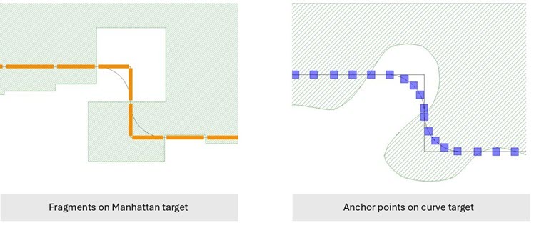
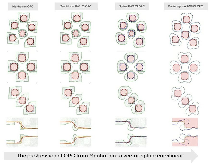
The physics of photolithography demonstrates that light exposure, diffraction, and resist interactions naturally produce curved pattern edges on silicon. Rigid, Manhattan-style corrections often lead to increased EPE, process variability, and ultimately, device performance penalties (figure 1).
Data complexity and optical proximity correction: Challenges for advanced photomask design
The transition to curvilinear OPC presents transformational opportunities – and some daunting new challenges – for mask data preparation, mask writing and OPC engineering. Traditionally, OPC uses a technique called fragmentation to break mask edges into discrete, optimizable segments.
With Manhattan layouts, the number of fragments is manageable and corrections can be applied efficiently. Curvilinear designs, on the other hand, exponentially increase the number of segments (or fragments) required to describe each mask edge (figure 2). This surge leads to:
- Explosive growth in mask data volume
- Increased simulation and OPC processing times
- Complicated mask writing and inspection flows
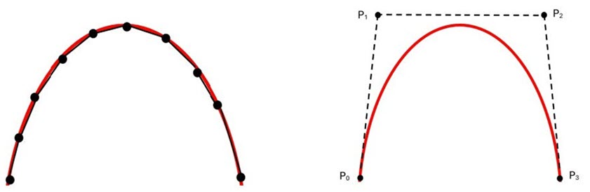
In a piecewise-linear (PWL) representation (left), a smooth curve must be approximated using many short linear segments and therefore requires many vertices. In contrast, a piecewise-Bézier (PWB) representation (right) can describe the same smooth curve using a single Bézier segment defined by only four control points P 0 – P 3. This significantly reduces geometric fragmentation and the number of parameters required to represent curvilinear mask shapes.
Vector-based mask correction: Optimizing curvilinear OPC with site-anchor decoupling
Overcoming these computational barriers requires a radical revision of mask modeling and data optimization. The traditional curvilinear OPC process is illustrated in figure 3. The anchor points and lines have a 1:1 mapping. Many legacy OPC flows cannot keep pace when every curve, arc or irregular feature must be discretized into thousands of points. The resulting bottlenecks threaten to outweigh the gains from higher pattern fidelity.
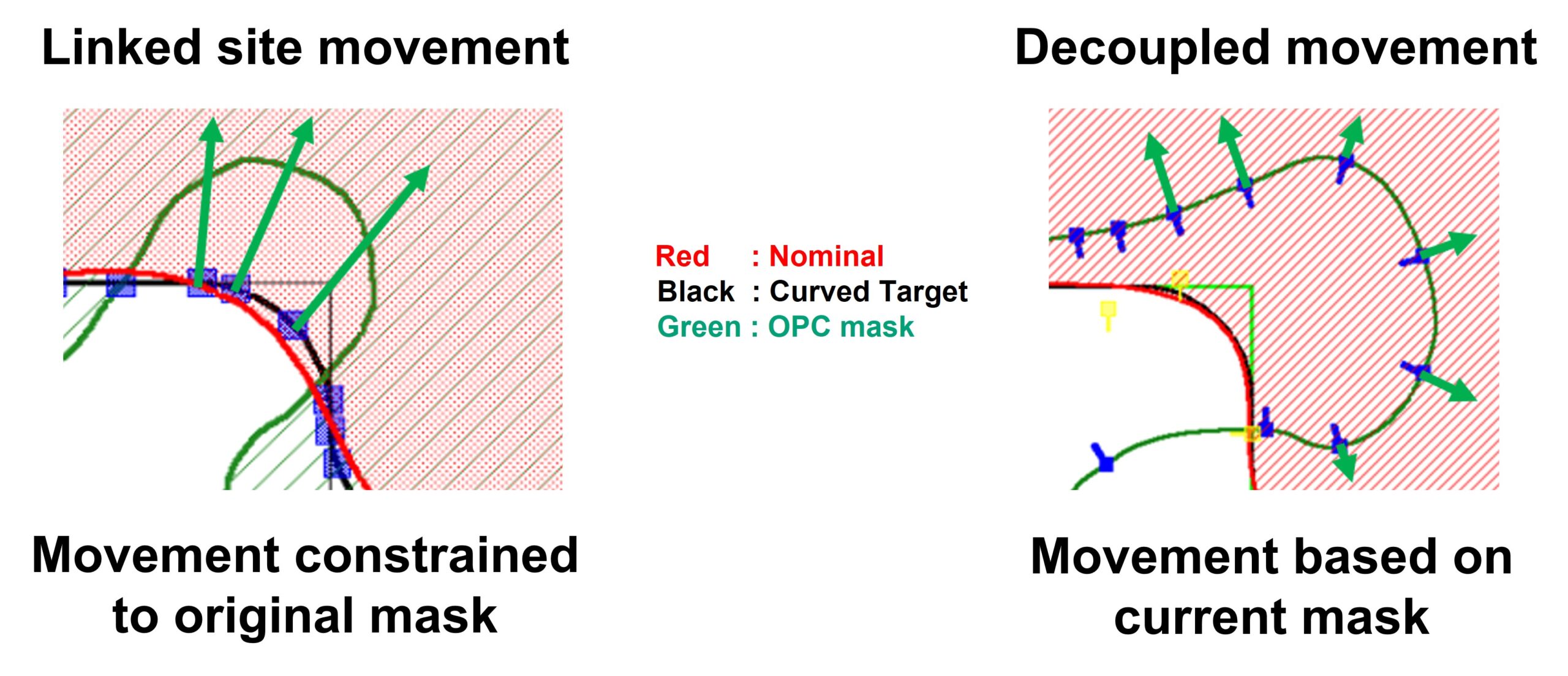
Figure 3. Widening the solution space through decoupled site movement.
A vector-based mask correction framework with site-anchor decoupling addresses these challenges directly. Instead of treating every mask edge fragment as both an optimization point and a correction site, this approach separates their roles:
- Optimization sites: Specific locations along the mask edge that are evaluated for pattern accuracy, EPE (edge placement error) or process sensitivity.
- Anchor points: Discrete mask control points used to guide and apply geometric corrections.
As illustrated in figure 4, anchor-site decoupling allows for the dynamic addition, removal or adjustment of anchor points throughout the optimization process. This flexibility lets the system de-fragment regions that converge rapidly, simplifying mask data, while simultaneously allocating additional sites or anchor points to areas with persistent EPE issues. Furthermore, anchor clustering prioritizes optimization in critical zones like tip regions, corners and dense curvilinear arcs, where process window robustness is most vulnerable.
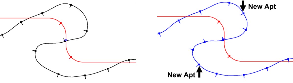
Decoupling sites and anchors lets OPC algorithms be both data-efficient and accuracy-driven. Rather than blanketing the entire mask with high-density correction points, computational resources can be directed precisely where they are needed – at regions with tight pitches, sharp bends or lithography hotspots.
This methodology allows the mask layout to be described in mathematical terms (such as Bézier splines and vectors), providing:
- Flexible, native handling of smooth curves
- Reduced overall data size
- Dynamic, locally adaptive correction strategies
- Efficient scaling for full-reticle, multi-layer designs
Edge placement error reduction: Real-world validation in advanced semiconductor manufacturing
No new technology is proven until it’s working in the foundry. Curvilinear OPC is already delivering measurable benefits in high-volume manufacturing across logic and memory fabs working at the most advanced nodes.
Unlike legacy approaches, which struggle with both runtime and excess data size, the site-anchor decoupling strategy has demonstrated:
- Tighter EPE control and improved yield
- Reduced process window variability
- Agile, faster mask recipe development
- Manageable data sizes that accelerate OPC cycles
Recent industry collaborations published technical results and deployment case studies at leading foundries underscore that the benefits of curvilinear OPC are already being realized (figure 5).
A significant advantage of this approach is that even a sparse anchor point density, which dramatically reduces file size, delivers superior edge placement error (EPE) results compared to traditional Manhattan OPC (figure 6).
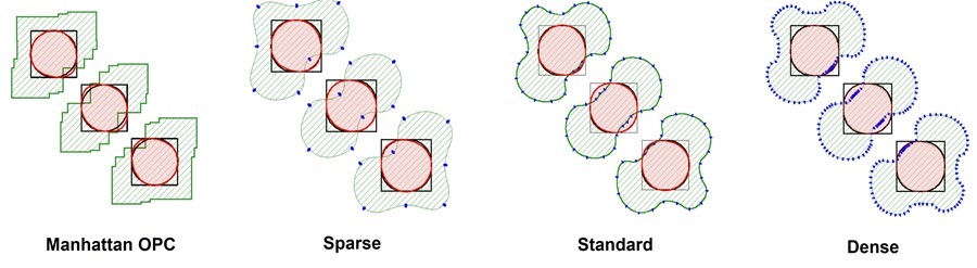
Comparison of Manhattan OPC and curvilinear OPC with sparse, standard, and dense anchor point configurations for a synthetic via pattern. Increasing anchor point density provides incremental improvements in edge placement error (EPE) at the expense of larger data size. Sparse anchor placement achieves a favorable balance between correction accuracy and data efficiency, demonstrating that high-quality curvilinear OPC does not necessarily require dense anchor point distributions.
Results of vector-based curvilinear OPC include:
- Improved pattern fidelity through true-to-physics mask geometries
- Lower edge placement error, boosting device yield
- More compact and manageable mask data
- Fast, scalable OPC and recipe tuning
- Enhanced printability for advanced process layers
- Robust support for complex, multi-patterned layouts
- Seamless integration with existing curvilinear mask flows
Industry collaboration and the future of curvilinear OPC in mask design
Momentum is rapidly building as the ecosystem aligns around curvilinear OPC and mask data innovations. Industry leaders, including EDA suppliers, foundries, memory manufacturers and research institutions, are actively collaborating to accelerate adoption of these novel approaches. The transition is no longer a question of “if,” but “how broadly and how soon.”
Publications, technical conferences and shared research underscore a simple truth: Vector-based mask correction and site-anchor decoupling are paving the way for future generations of semiconductor device manufacturing.
Curvilinear OPC sets the new standard for semiconductor mask optimization
As semiconductor technology grows ever more complex, the gap between digital design intent and manufacturable masks can be closed only by aligning with the underlying physics and by harnessing new, efficient computational techniques. Through curvilinear OPC and the innovation of vector-based site and anchor decoupling, the industry gains the precision, efficiency and yield needed for next-generation electronic devices.
These innovations tackle today’s bottlenecks and lay the foundation for tomorrow’s advances in photomask technology, OPC and semiconductor manufacturing.
For further reading:
Optimizing curvilinear OPC: Vector-based site and anchor decoupling [https://resources.sw.siemens.com/en-US/white-paper-optimizing-curvilinear-opc-vector-based-site-and-anchor-decoupling/]
Sagar Saxena is a Senior Product Engineer at Siemens EDA specializing in computational lithography, Optical Proximity Correction (OPC), and advanced patterning solutions for leading-edge semiconductor manufacturing. With nearly a decade of experience in semiconductor design and manufacturing software, Sagar has led the development and deployment of advanced OPC technologies, including curvilinear OPC methodologies, computational lithography workflows, and next-generation mask synthesis solutions. His work has contributed to high-volume manufacturing enablement at advanced nodes for some of the world’s most advanced semiconductor processes.
Also Read:
Reimagining 3D IC Design: From Architecture to Signoff
Agentic AI accelerates 3D IC engineering for the AI factory era
Siemens and NVIDIA Accelerate Lithography for Next-Generation AI Chips
Share this post via:


Comments
There are no comments yet.
You must register or log in to view/post comments.