





By Bhanu Pandey
The semiconductor industry is currently facing a significant challenge in functional verification. According to the most recent Wilson Research Group / Siemens EDA Functional Verification Study, first-silicon success rates have hit a historic low, with nearly 68% of designs requiring two or more spins. While digital verification has matured with robust formal methods and constrained-random testing, analog and mixed-signal (AMS) verification remains a primary source of these re-spins.
One of the most elusive and damaging defects in the AMS domain is the “floating net.” As designs move toward advanced process nodes and increasingly aggressive power management strategies, the risk posed by these structural defects has grown from a niche concern to a critical reliability bottleneck.
The anatomy of a floating net
In modern integrated circuits, power-down modes are essential for extending battery life and managing thermal envelopes. Designers implement these modes by using MOSFET switches to disconnect bias currents and power supplies from specific analog IP blocks—such as LDOs, amplifiers, or PLLs—when they are not in use.
A floating net occurs when a circuit node is disconnected from all low-impedance paths to a defined voltage (supply or ground). In a power-down state, the voltage on this node is no longer actively driven; instead, it is determined by the trapped charge on parasitic capacitances. Figure 1 shows a top level schematic of a CMOS LDO voltage regulator with a standard enable/disable function
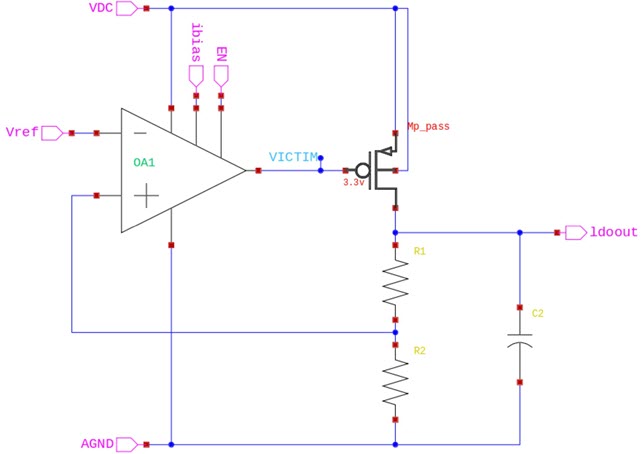
Because no node is perfectly isolated, leakage currents through the surrounding transistors will cause the voltage on this floating net to drift over time. This drift is the “silent killer.” If the voltage reaches the threshold of a connected transistor, it can inadvertently turn that device on. This can trigger a cascade of failures: unregulated power routing, latch-up conditions, or even permanent physical damage to the device or downstream components.
Why SPICE is blind to structural defects
For decades, SPICE simulation has been the gold standard for analog verification. However, when it comes to floating nets, SPICE has a massive blind spot. There are three primary reasons why even the most rigorous simulation testbenches fail to catch these defects.
- The convergence artifact SPICE simulators are designed to find a numerical solution for circuit equations. When a simulator encounters a truly floating node, the matrix becomes singular, and the simulation fails to converge. To prevent this, simulators often use a technique called “gmin stepping,” which adds a very high-impedance resistor (typically ohms) from every node to ground. While this allows the simulation to complete, it inadvertently masks the floating net by providing a path to ground that does not exist in the actual silicon.
- The time-scale problem Floating net failures are often time-dependent. A node might take milliseconds or even seconds to drift to a critical voltage level. Standard functional simulations rarely run for this duration, as the computational cost would be prohibitive. Consequently, the defect remains hidden during the short windows typically analyzed during verification.
- Testbench coverage Detecting a floating net requires testing every possible combination of power-down states and sequences. In a complex SoC with dozens of power domains, the number of permutations is astronomical. It is statistically impossible to cover all these conditions using transient simulation alone.
The “VICTIM” net: A case study in failure
Consider a common scenario in a high-performance analog block. An enable signal () controls the power state of the block. When is low, the paths to both the supply () and ground () are cut to eliminate static power consumption.
In one analyzed design, a specific net—internally labeled the “VICTIM” net—connected to the gate of a large PMOS pass transistor. When the block was enabled, the net was driven correctly. However, in power-down mode, the net was left entirely floating (Figure 2).
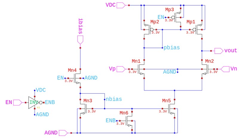
During simulation, the defect was masked by the simulator’s internal grounding. But in silicon, the trapped charge on the gate caused the pass transistor to partially turn on during a long idle period. This resulted in a massive current spike that damaged the output stage, leading to a costly field failure and a subsequent re-spin.
Shifting reliability left with structural analysis
To address the limitations of simulation, the industry is moving toward automated structural analysis. Tools like the Calibre Insight Analyzer allow designers to “shift-left” their reliability verification by identifying structural defects based on the circuit’s topology rather than its transient behavior.
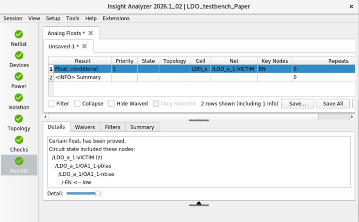
Structural analysis works by parsing the netlist and layout to build a complete map of the circuit’s connectivity. It then evaluates this map against all defined power modes. Unlike SPICE, which looks for functional output, structural analysis looks for the absence of a valid state (Figure 3).
How to catch floating nets that simulation misses
Finding floating nets requires the use of a layout-aware circuit integrity analysis tool. For example, the Calibre Insight Analyzer tool doesn’t just look at the schematic; it accounts for the physical parasitics that contribute to charge trapping and drift. The tool follows a structured three-step process:
- Mode definition: The user defines the various power states of the design, including which signals are high, low, or high-impedance in each mode.
- Topological checking: The tool traverses the circuit graph to identify any node that lacks a low-impedance path to a supply or ground in any given mode.
- Reporting and visualization: Discrepancies are flagged and cross-probed back to the layout and schematic, allowing designers to quickly implement a fix—such as adding a high-impedance bleeder resistor or a tie-off cell.
The path to signoff confidence
As we move toward 3D IC architectures and heterogeneous integration, the complexity of power delivery networks will only increase. The interdependencies between thermal profiles, mechanical stress, and electrical reliability mean that a single floating net can have catastrophic system-level consequences.
Relying on legacy verification methods is no longer sufficient. Automated structural analysis is becoming a mandatory requirement for analog signoff. By integrating these checks early in the design cycle, engineering teams can move beyond the “silicon success crisis” and deliver high-performance, reliable products with confidence.
Conclusion: Moving from transient simulation to structural signoff
Floating nets are a structural reality of modern low-power design, but they don’t have to be a reliability risk. By understanding the limitations of SPICE and adopting automated structural analysis, designers can identify these silent killers before they ever reach the fab. Shifting reliability left isn’t just a best practice – it’s the only way to ensure silicon success in the advanced node era.
About Bhanu Pandey:
Bhanu Pandey is a product engineer for Calibre Design Solutions at Siemens Digital Industries Software, with responsibility for the Insight Analyzer circuit reliability analysis tool. His focus and technical experience are in analog circuits.
Also Read:
Siemens and TSMC push AI deeper into chip design
From Custom Silicon to AI Systems: Why Cross-Layer Engineering Matters
The Invisible Bottleneck Is Costing You Time You Can’t Get Back
Share this post via:



Comments
There are no comments yet.
You must register or log in to view/post comments.