The Tale of Three Metrics
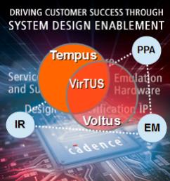 Meeting PPA (Performance, Power and Area) target is key to a successful design tapeout. These mainstream QoR (Quality of Results) metrics are rather empirical yet inter-correlated and have been expanded to be linked with other metrics such as yield, cost and reliability. While the recent CPU performance race is less intense as Moore’s Law based scaling is increasingly costlier and more complex, power is taking the center stage. This has been intensified by the proliferation of more silicon geared toward addressing mobility (automotive, wireless-augmented- anything), distributed applications (Internet-of-Things) or scalable computing (multi-core).
Many of the adopted low-power implementation flows have shown that a holistic approach is necessary in order to achieve an optimal power target. It must also be initiated early at the architectural level such as addressing multiple power domains and clock domain partitioning, followed by power optimization at different level of the implementation stages. Concurrently, an accurate power analysis is required to provide feedback for needed adjustments to the optimization constraints as tradeoff recurrences are expected among these metrics.
Power Signoff Challenges
Power signoff checks power integrity of the grid. According to Jerry Zhao, Cadence Product Director, today designs can be categorized into two types for the purpose of analyzing the power grid constructions and identifying its challenges. The first design type demands capacity as it contains billions of instances and nodes such as the power-hungry oriented GPUs (Graphical Processing Unit) or CPUs for machine learning. The other is small in size but more sophisticated, which requires multiple power domains (such as IoT related chips) or special needs (such as packaging integrated analysis for automotive) –for this type, a higher analysis accuracy is needed.
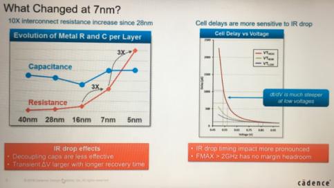
Additionally, with the advanced nodes such as 7nm and 5nm FinFETs where metal resistance is more pervasive, higher correlation accuracy is also required between the implementation estimates and the analysis results generated by the signoff tools. In flow utilizing a traditional signoff approach, non-converging iterations are common occurrences as it relies on the use of design margins as well as due to a disconnect in either the underlying data model or the optimization/analysis engine of the associated point tools.
Cadence True Signoff Solution
As part of a tapeout signoff, design teams perform various validation including physically related verification (DRC, LVS, reliability), timing and power. While it is common to have crosstalk and SI (Signal Integrity) effects concurrently done with timing analysis, power verification (related to IR drop, electromigration/EM) is traditionally decoupled from timing analysis, in spite of the fact that an IR induced lower power biasing and the remedy to an EM avoidance may incur significant timing differentials that could change the criticality of a timing path.
Driven by such tighter correlation needs especially in the advanced nodes domain, Cadence launched project Virtus (Voltus IR drop TempUS technology) which integrates the power and timing analysis to yield a true signoff solution. It had also been aligned with the existing Cadence digital implementation flow for both QoR predictability and convergence. The overall solution is dubbed full-flow digital.
As discussed during Cooley’s DAC 2018 Troublemaker Panel, Jerry shared a customer case involving a high frequency design. The 3Ghz design passed signoff using other third party power and timing tools, but failed to perform on silicon at the targeted frequency by several hundreds of Mhz. This design was then subjected to true signoff analysis, which was able to uncover the presence of IR drop violations that could induce timing violations comparable to the earlier post-silicon observation.
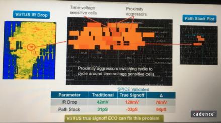
How much impact does an IR drop violation have on timing? At the DAC theater presentation, Cadence showcased such IR induced timing violations on a 2.5Ghz, 7nm CPU based design testcase. A non-critical path having +31ps slack and passing power integrity analysis with +42mV margin, was identified with true signoff as failing timing by -33ps due to the presence of proximity aggressors (equivalent to a 8% slow down in speed). This path interestingly was not one of the top-paths, instead, it was buried in the deeper non-critical path bin.
Speed and Parallelism
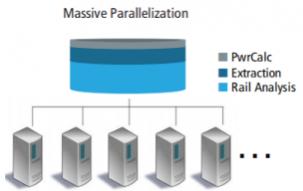
Since scalability and performance are needed for power integrity analysis, Cadence has recently rolled-out Voltus-XP, enhanced with extensive parallelism algorithm to support power grid signoff on giga-scale designs with massively distributed processing. It is cloud ready and provides up to 5x speedup.
Full-Flow Digital Solution
The tight handshake exemplified between Voltus and Tempus seems to be just one of the many close interactions among Cadence tools as shown in Full-Flow Digital Solution diagram, which is inline with this year Cadence’s slogan of being a system design enabler.
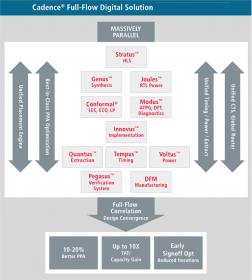
“Design closure is tightly correlated with how a cell is placed and routed as it impacts how current flows through the placed region and thus, influencing the IR drop,” stated Jerry referring to Voltus-Innovus IR-drop-aware placement fixing.
As one move towards the top of the die, packaging has its own IR drop requirements that are different than chip level. It is more thermal centric and involves gradual change compared with quick voltage ramp. A similar handshake with packaging analysis is also needed. Designer is expected to iterate through the tools in the ecosystem though not required to be concurrent, in order to ensure a QoR convergence.
In addition to IR drop check, for 7nm and 5nm power integrity, meeting foundry driven EM rules requires a year-round team collaboration which culminates in passing foundry certification process.
Signoff Solution for The Advanced Nodes
Asked on his take with the adequacy of Cadence current tool offerings for 7nm or 5nm signoff, Jerry stated that implementation step could further leverage the analysis outcome. “When Voltus is running it will report hot-spot areas (i.e. with IR drop error) understood by Innovus and used to do IR aware placement fixing,” stated Jerry. The tool is smart enough to move the aggressor by a few rows based on a cost function. A rerun of Voltus is needed to ensure it is fixed. Using such approach designer can reduce the IR drop by 30% in one iteration. With multiple iterations, it would resolve significant number of IR related issues although it may not fix the whole problems as there are some designer imposed constraints such as not allowing tool to touch the clock trees.
Addressing it from another angle has been demonstrated through the use of Tempus timing signoff tool. Jerry said that as Voltus and Innovus shared the same database (data model), an integrated Tempus-Voltus timing analysis can be done and an ECO based on voltage report can be generated to fix timing violations.
To recap, both timing and power signoffs have become increasingly longer with more complex designs and advanced nodes. Cadence integrated signoff solution not only provides multi-dimensional analysis but also a tightly coupled solution with the optimization based tools to alleviate signoff bottlenecks.
For more info on Voltus please check HEREand Cadence silicon signoff HERE
Share this post via:


Comments
2 Replies to “A True Signoff for 7nm and Beyond”
You must register or log in to view/post comments.