In case you missed the TSMC event, ANSYS and TSMC are going to reprise a very important topic – signing-off reliability for ADAS and semi-autonomous /autonomous systems. This topic hasn’t had a lot of media attention amid the glamor and glitz of what might be possible in driverless cars. But it now seems like the cold light of real engineering needs are advancing over the hype, if this year’s CES is any indication (see my previous blog on CES). Part of that engineering reality is ensuring not only that we can build these clever systems but that they will also continue to work for a respectable amount of time; in other words that they will be reliable, a topic as relevant for today’s advanced automotive electronics as it is for the systems of tomorrow.
REGISTER HERE for this event on February 22nd at 8am Pacific Time
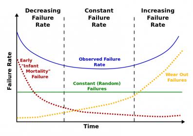
This topic is becoming a pressing concern, especially for FinFET-based designs. There are multiple issues impacting aging, stress and other factors. Just one root-cause should by now be well-known – the self-heating problem in FinFET devices. In planar devices, heat generated inside a transistor can escape largely through the substrate. But in a FinFET, dielectric is wrapped around the fin structure and, since dielectrics generally are poor thermal conductors, heat can’t as easily escape leading to a local temperature increase, and will ultimately escape significantly through local interconnect leading to additional heating in that interconnect. Add to that increased Joule heating thanks to higher drive and thinner interconnect and you can see why reliability becomes important.
ANSYS has developed an amazingly comprehensive range of solutions for design for reliability, spanning thermal, EM, ESD, EMC, stress and aging concerns. In building solutions like this, they work very closely with TSMC, so much so that they got three partner of the year awards at the most recent TSMC OIP conference!
Incidentally my CES-related blog is here: https://www.legacy.semiwiki.com/forum/content/7274-ces-exhibitor-s-takeaway.html
Summary
Design for reliability is a key consideration for the successful use of next-generation systems-on-chip (SoCs) in ADAS, infotainment and other critical automotive electronics systems. The SoCs manufactured with TSMC’s 16FFC process are advanced multicore designs with significantly higher levels of integration, functionality and operating speed. These SoCs must meet the rigorous requirements for automotive electronics functional safety and reliability.
Working together, ANSYS and TSMC have defined workflows that enable electromigration, thermal and ESD verification and signoff across the design chain (IP to SoC to package to system). Within the comprehensive workflows, multiphysics simulations capture the various failure mechanisms and provide signoff confidence not only to guarantee first-time product success, but also to ensure regulatory compliance.
Attend this ANSYS and TSMC webinar to learn about ANSYS’ chip-package-system reliability signoff solutions for creating robust and reliable electronics systems for next-generation automotive applications, and to explore case studies based on TSMC’s N16FFC technology.
Founded in 1970, ANSYS employs nearly 3,000 professionals, many of whom are expert M.S. and Ph.D.-level engineers in finite element analysis, computational fluid dynamics, electronics, semiconductors, embedded software and design optimization. Our exceptional staff is passionate about pushing the limits of world-class simulation technology so our customers can turn their design concepts into successful, innovative products faster and at lower cost. As a measure of our success in attaining these goals, ANSYS has been recognized as one of the world’s most innovative companies by prestigious publications such as Bloomberg Businessweek and FORTUNE magazines.
For more information, view the ANSYS corporate brochure.