I’ve been driving cars since 1975 and in the early days we had simplistic gauges for feedback like: Speed, Fuel level, Oil level, RPM. Back then when you popped the hood of a car you could see through the engine compartment onto the ground below, however with today’s cars the engine compartments are crammed with tubes, wires and assemblies packed so tightly that you cannot see the ground and electronic content abounds. Dashboards of modern cars even report when a turn signal or other light bulb is burnt out or if the tire pressure is out of spec and needs to be checked. A report from IDCpredicts a 19% growth rate for infotainment systems in our cars. McKinsey sees automotive semiconductor trends in several areas:
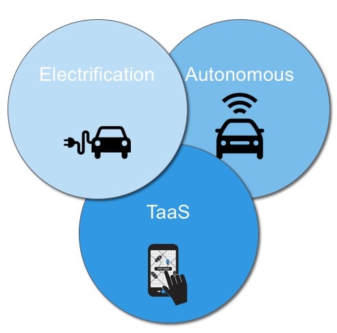
- Vehicle electrification
- Increased connectivity
- Autonomous driving
- Shared mobility services
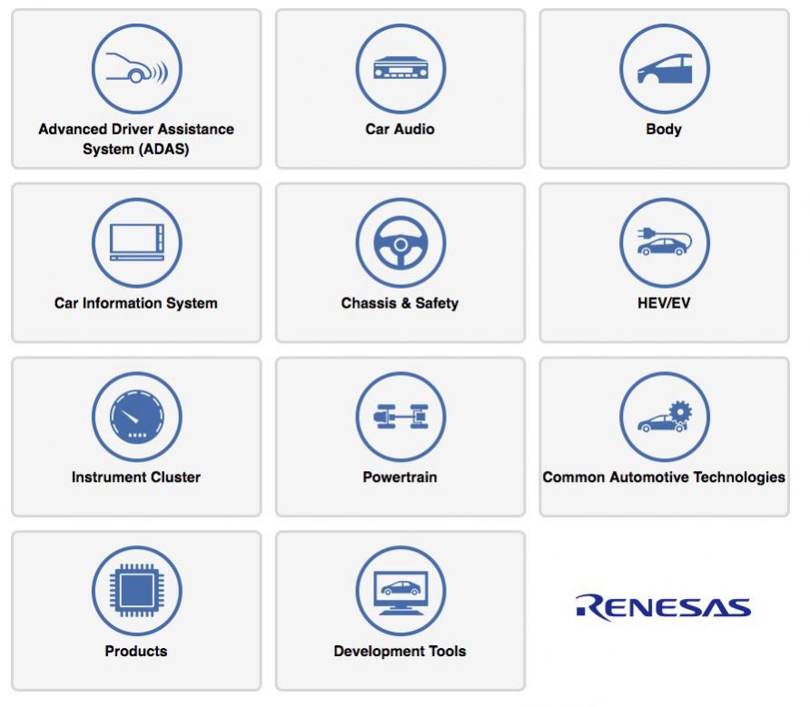
One established vendor to the automotive industry over the years has been Renesas, offering products in eleven distinct areas:
So a big challenge in automotive electronics is safety, we want to know that our cars are operating safely and furthermore we want to know when something has gone wrong so that we can take action like schedule maintenance or repairs. To accomplish these goals our semiconductor suppliers do extensive testing of electronic parts before they are shipped to automotive vendors, but what about after the parts are installed in the vehicle? Is there a way to test some or all of the electronic components in our cars throughout the lifetime of use?
The short answer is yes, there are techniques that chip designers can employ to allow testing of electronics that are installed, or in-system testing. We love our acronyms in high tech so I’ll give you another one that fits our topic and it’s called BIST, which stand for Built In Self Test. With BIST the chip designer adds some extra logic inside their IC that will:
- Check itself at power-up for faults
- Check for conditions that cause failures
- Report the issue(s)
An ideal BIST approach would be one that provides high fault coverage of all gates inside the IC, and does so in a short amount of time like milliseconds. EDA tools have come to automate adding the BIST logic to a chip so that a designer doesn’t have to manually figure out the best implementation, and engineers at Renesas have just publicly talked about how they used the DFTMAX LogicBISTtool from Synopsys in their automotive group. From a design engineer perspective you add LogicBIST when your RTL code is stable and before physical implementation as shown in the following BIST flow:
During the process of adding LogicBIST the Renesas engineers also used a tool to increase fault coverage levels called SpyGlass DFT ADV that accepts RTL code, ensures the design is scan compliant, diagnoses DFT issues early, does lint checking and DFT analysis and estimates stuck-at and transition faults:
Renesas and Synopsys were able to certify DFTMAX LogicBIST was meeting Part 8 of the ISO 26262 functional safety standard, something that the automotive industry regulates.
Benefits that Akira Omichi from Renesas sees from this LogicBIST approach include:
- Useful on mixed-signal automotive designs
- Power-on Self Test (POST) improves safety
- Consumes minimal chip area
- Gives high fault coverage on the digital logic
- Easy to use
Talking with Robert Ruiz of Synopsys by phone I learned that the ISO 26262 standard for functional safety presumes that there is a human driver in the car, so it doesn’t directly pertain to fully autonomous vehicles. With POST and LogicBIST the goal is to find and report any latent faults, typically showing up as a message on the dashboard.
Over time you can expect to see more and more automotive semiconductor suppliers to add LogicBIST to their IC designs as a means to improve functional safety and differentiate their product offerings. With EDA vendors like Synopsys it’s an easier process for chip designers to add LogicBIST because of the automation in their DFTMAX LogicBIST tool.
Related blogs: