As I have said many times, IEDM is one of the premier conferences for semiconductor technology. On Sunday before the formal conference started I took the “Boosting Performance, Ensuring Reliability, Managing Variation in sub-5nm CMOS” short course. The second module in the course was “Multi-Vt Engineering and Gate Performance Control for Advanced FinFET Architecture” taught by Steven Hung of Applied Materials. This excellent module was particularly timely because GLOBALFOUNDRIES and Intel gave papers on their 7nm and 10nm processes at IEDM and both processes use work function metals to control threshold voltages. In this article I will discuss this emerging process technology.
Introduction
Simply put, the threshold voltage (Vt) of a MOSFET is the voltage that is required to turn the transistor on. As optimization of power and performance have become increasingly important for mobile devices, the number of different threshold voltages available on a process have proliferated. Where one or two threshold voltages were once typical, today we are seeing four or even five threshold voltages. Multiple threshold voltages allow designers to select the best option for each section of a design trading-off power and performance.
Setting Threshold Voltage (Vt)
The Vt of a MOSFET is determined by:
- Interface charges – because interface charges can vary over time due to traps charging and discharging, it is generally desirable to minimize interface charges and they are not used to “tune” the threshold voltage.
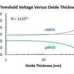
- Gate dielectric (oxide) thickness – Vt varies with gate oxide thickness with Vt being reduced for thinner oxides, see figure 1. For current foundry processes, it is common to have two oxide thicknesses and sometimes three. A thinner oxide may be used in the core for low Vt – high performance transistors and a thicker oxide may be used in the I/O area to support higher voltages.
Figure 1. Threshold voltage versus oxide thickness at a fixed channel doping level.
- Channel doping – for many years the main method of producing multiple Vts on the same process has been to use masked implants to dope selected channel regions. Figure 2 illustrates Vt versus channel doping. There are two main issues with channel doping to set Vts. The first is that doping the channel reduces mobility and performance. Secondly, at very small dimensions there are only a few dopant atoms in the channels and small changes in the number of dopants referred to as random dopant fluctuations (RDF) can lead to variations in Vt.
Figure 2. Threshold voltage versus channel doping at a fixed oxide thickness.
- Work function – since the transition to high-k gate oxides occurred, metal gate electrodes have been used to avoid the polysilicon depletion effect. The high-k metal gate (HKMG) process typically has two types of gate electrode metal stacks, one for the pFET and one for the nFET. The dual work function metals (WFM) is part of optimizing the nFET and pFET Vts. Now we are seeing more than two WFM used to “tune” Vt. With the advent of the foundry 7nm processes (Intel 10nm process) we are seeing multiple WFMs used to tune Vts with no channel doping. This approach improves mobility in the channel and therefore performance and avoids RDF.
High-k Metal Gates
In the early days of HKMG there were two approaches, gate-first and replacement metal gate (RMG). In gate first the HKMG is formed before the transistor implants, anneals and raised source/drains. The problem with this process is that the HKMG structure must stand up to a lot of high temperature processing and achieving optimal Vts is very difficult. RMG has now become the standard HKMG process.
In an early version of RMG, an interfacial oxide, high-k gate oxide and capping layer are deposited and then covered with a sacrificial polysilicon layer. The transistor implants, anneals and raised source/drains are performed. The sacrificial polysilicon is then etched out and gate WFM are deposited. This avoids the WFMs seeing a lot of high temperatures. In the current versions of this process an interfacial oxide is grown, sacrificial polysilicon is deposited and then the transistor is formed. The sacrificial polysilicon is etched-out, the surface is cleaned and then the interfacial oxide, high-k oxide, capping titanium nitride (TiN) layer and second sacrificial polysilicon layers are deposited. An anneal of the high-k oxide is preformed and the second sacrificial polysilicon layers is etched away. The WFM is now deposited. This method avoids having the high-k oxide exposed to all the high temperature transistor formation process steps.
Two Work Function Metals
For many years the standard WFM process has been to create an n and a p WFM.
The basic process is (does not include second sacrificial polysilicon deposition, anneal and removal), see also figure 3:
- Form interfacial oxide
- Deposit high-k gate oxide
- Deposit TiN cap layer
- Deposit tantalum nitride (TaN) etch stop layer
- Deposit TN work function layer
- Mask and etch TiN off of nFET
- Deposit titanium aluminum carbon (TiAlC) work function layer
- Deposit TiN barrier
- Deposit tungsten (W) fill
- Planarise
Figure 3. Dual work function metals.
It should be noted that although this stack is shown flat for illustrative purposes, the films are deposited into a trench.
Four Work Function Metals
At 10nm TSMC implemented the first four WFM approach I have seen. In the process outlined below the net result is two nFET WFM stacks and two pFET WFM stacks. This would achieve two Vts and I believe channel doping is used to achieve additional Vts. Possibly there would be one nFET and one pFET with undoped channels for maximum performance and then perhaps three additional Vts with doping.
The basic process is (does not include second sacrificial polysilicon deposition, anneal and removal), see also figure 4:
- Form interfacial oxide
- Deposit high-k gate oxide
- Deposit TiN cap layer
- Deposit tantalum nitride (TaN) etch stop layer
- Deposit TN work function layer
- Mask and etch TiN off of everything but the high Vt pFET
- Deposit second TaN layer
- Mask and etch TaN2 off of the low Vt nFET and high Vt pFET
- Deposit TiAlC work function layer
- Mask and etch TiAlC off of the low Vt pFET
- Deposit TiN barrier
- Deposit tungsten (W) fill
- Planarise
Figure 4. Four work function metals.
This process flow was developed after examining cross sections of 10nm TSMC process provided by TechInsights.
If only two Vts are required, this 4 WFM process will meet that requirement. If channel doping is acceptable, then implants may be used to provide additional Vts.
For the Intel 10nm process (similar to foundry 7nm) Intel has a base process with 2 Vts achieved with 4 WFMs and an optional 3 Vt process achieved with 6 WFMs. GLOBALFOUNDRIES 7nm process has 4 Vts achieved with 8 WFMs. These processes are not available for analysis yet and we don’t know how these 6 and 8 WFM stacks are achieved. In the next section I will discuss some of the options.
Multiple Work Function Metal Options
Multiple work function can be achieved by simply using different metals that have different work functions, but there are a limited number of suitable metals.
In the “Multi-Vt Engineering and Gate Performance Control for Advanced FinFET Architecture: module of the short course I took, three ways of modifying work functions were discussed:
[LIST=1]
- Thickness modification – changing the thickness of work function metals layers changes the work function. This allows changes in the Vt over a wide range but requires multiple depositions, masks and etches and very tight thickness control. This technique results in stacks of different thicknesses and may be difficult to implement for gate-all-around.
- Material modification – this technique introduces or removes species such as oxygen to change Vt. This technique has less range of values than thickness modification and is most effective when the layers are closer to the high-k gate oxide. This technique does not result in different thickness for each WFM stack. One technique that has been investigated for material modification is implanting nitrogen into the WFM, the concern with this technique is the implanted ions may knock metal atoms from the WFM into the high-k gate oxide.
- Electrostatic dipole – certain elements can introduce a dipole into the high-k gate oxide, for example elements such a lanthanum (La). Dipole formation with La and aluminum (Al) was used by the IBM/GLOBALFOUNDRIES/Samsung alliance as part of their WFM scheme for their gate first process at 28nm. This technique offers a broad range of Vts but needs very good thickness control of the deposited dipole materials and thermal drive in.Conclusion
The transition to fully undoped channels with WFM Vt control is underway. TSMC has implemented 4 WFM at 10nm, Intel ‘s 10nm (similar to foundry 7nm) will feature 4 and 6 WFM options and GLOBALFOUDNRIES 7nm will have 8 WFM. We don’t yet know how this many WFMs will be achieved but likely it will be a combination of the techniques outline in the preceding section.The change to undoped channels should improve performance and reduce Vt variations enabling lower voltage operation for lower power.