The complexity of an SoC design necessitates that the project managers have accurate visibility into the overall design status, spanning the entire range of tasks – from functional simulation error triage, to physical layout verification errors, to electrical analysis results. Flow scripts used by SoC teams parse the log file data generated by the underlying EDA tools invoked, to capture the status of each design block. These output results are stored in a database, from which a project scoreboard application pulls information for a view into the complete project snapshot (and history).
Given the variety of flows and the disparate nature of EDA vendor tool log file data for each flow, scoreboard development (and maintenance) for an SoC project requires significant CAD team resources. The scoreboard application includes detailed design revision and methodology dependency checking, as well – as project version updates are applied to ongoing design releases, the scoreboard database needs to ensure flows are re-executed and old results invalidated. The CAD and methodology teams collaborate to capture the flow dependency criteria. In return for the CAD team resource investment, the scoreboard information is extremely valuable, as it provides insights into SoC project schedule milestone risks and areas where design engineering resource re-balancing may be needed.
Another key SoC application is issues management, often simply referred to as the bug tracking tool. The issues application utilizes another database, with a rich and diverse set of information to be stored and queried – e.g., text, graphics, issue priority, issue owner, reviewers, approvals required to close, date opened, target close date, design block(s) impacted, related specifications, model build configuration (with all version tags), etc. This information evolves over time, as the investigation of the issue results in comments, proposals, dependencies on other issues, and a resolution recommendation that will need to be reviewed/approved/implemented/verified.
Both commercial and open-source issues management applications are available, and have been adopted by SoC teams. Often, a tool developed for software defect management will be adapted by the CAD team for the specific requirements of an SoC design.
Scoreboard and issues tracking tools are a fundamental aspect of any SoC design project management activity. PCB design projects have comparable tracking requirements, and some unique characteristics. The PCB project involves a broad cross-section of teams involved in design reviews – especially, component qualification engineering and component procurement. And, there is typically not a great deal of CAD resource available to develop and maintain scoreboard and issues applications for the PCB team. (Fortunately, there is less diversity in the EDA tool platform(s) used to capture, design, verify, and release the PCB data for manufacture.)
I recently had the opportunity to chat with Mark Hepburn, Product Management Director, System/Package/Board, in the Custom IC & PCB Group at Cadence, about project management tools for PCB designs. Mark highlighted, “We recognized the need for a broad set of users to obtain project metrics and analytics from the Allegro PCB platform. The users may not be actively working with Allegro, such as the project manager of a PCB design, or the Supply Chain Management organization overseeing multiple designs. We recently introduced Allegro Pulse, an enterprise-grade server database environment, with web portal views into different project tracking applications.”
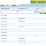
Mark shared a few screen shots from Allegro Pulse, for examples of the analytic data available. The figure below illustrates the Bill-of-Materials parts management view, which provides the supply chain group early visibility into the project BoM, with comparisons to preferred parts list libraries.
The screen shot below provides an example of a PCB project scoreboard view. (The full scoreboard web portal page is customizable.) The view may include metrics built-in to Pulse and custom metrics defined by users. The built-in metrics include the status of Allegro PCB checking tools – e.g., component placement and connectivity checking, electrical rules checks. The scoreboard view may also incorporate detailed analytics – e.g., pin complexity calculations.
The figure below illustrates the issues management application in Pulse, directly accessible by users from an Allegro toolbar pull down menu. The issues app includes features for database search, e-mail list notification, and a summary rollup into the scoreboard.
A general project management application is also provided in Pulse – the status of project tasks, schedule, progress toward schedule milestones, etc., is coordinated with the other apps.
The complexity of current PCB designs requires comparable project management tool support that SoC designs have employed. Allegro Pulse addresses that need with a suite of integrated, customizable PM applications.
For more information on Allegro Pulse, here are two links that may be of interest – the first link is the general product landing page (with a video), while the second link is an overview product description (.pdf file).
-chipguy