I recently read a new white paper release by Mentor, a Siemens Business, that delved into the intricacies of Chemical Mechanical Polishing (CMP) and I got a sense of Déjà vu. My professional career in the IC industry started at Texas instruments and the white paper made me think of a conversation I had with one of my colleagues over lunch. We were experiencing some yield issues and he told a story of getting home late and trying to explain to his spouse the problems we were encountering. We often take for granted the miracle that the manufacturing of ICs is, and my friend’s wife brought that fact into perspective when she quipped, “Forget about yield, you should be happy any of them work at all!”.
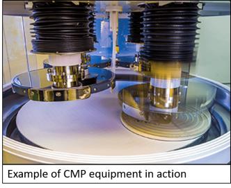
One of the true innovations that helped make the IC industry what it is, has been the use CMP. CMP is responsible for the “leveling” of the wafer layers that makes for a good planar process. The CMP process is fascinating as it’s roughly akin to running a disc sander with a chemical slurry over the wafer to “polish” it smooth. This polishing is highly dependent upon the materials being polished and the density and shapes of the materials in any given location of the chip. To get consistent (and therefore flat) polishing, it’s important to maintain a constant density balance across the chip to prevent bumps and dishing that can cause shorts and opens.
With the introduction of softer copper interconnect at the 130nm node (vs harder aluminum), and then the introduction of high-k metal-gate technologies with costlier lithographic patterning schemes, it has become increasingly important to have higher accuracy CMP models that can be used to identify possible design “CMP hot-spots” before going to manufacturing. As mentioned, Mentor recently released a new white paper with a novel approach that uses machine learning and neural networks to accelerate the generation of good post-deposition (pre-CMP) profiles to be used with CMP manufacturing simulation models.
The main concept for building a CMP model is to extract geometric pattern properties of the chip layout, generate a pre-CMP surface profile after numerous etch and deposition steps and then use that data to simulate the post-CMP surface profile for different patterns on the layout. For high-quality modeling, it’s important to have a set of models corresponding to the deposition processes used by manufacturers to generate the correct input profile for CMP equipment simulations.
Generation of a high-quality pre-CMP surface profile is crucial for accurate CMP modeling and is complicated due to the convolving of geometric data, different materials and both short and long-range effects. Building physics-based models for different types of depositions processes such as high-density plasma CVD (HDP-CVD) and spin-on dielectric (SOD), is challenging and isn’t practical for more exotic deposition flows such as flowable CVD (FCVD) and enhanced high-aspect-ratio processes (eHARP). The key here is that if the pre-CMP profile isn’t accurate then neither will be the results of the CMP simulations for the post-CMP profile.
To attack this problem, researchers at Mentor recently had the idea of using machine learning (ML) algorithms to do a sensitivity analysis of measurement data on post-deposition (pre-CMP) surface profiles and found that the profile dependency was primarily influenced by the underlying pattern geometries while long-range effects look to be more secondary. Armed with this information they proposed the idea of using neural network (NN) regression calculations to model the pre-CMP surface profile using as input the geometric characteristics of the underlying patterns. The output of the NN would be the estimate of the pre-CMP profile that would then be used as input for the CMP equipment modeling.
Mentor already has algorithms to extract local geometric pattern characteristics from their Calibre CMP ModelBuilder and Calibre CMPAnalyzer products. They used these tools to extract pattern information such as width, space, pattern density and geometry perimeter and fed this into a multi-layer NN to generate post-deposition surface profile height data predictions. To test the practicality and accuracy of using ML and NNs to generate CMP models, Mentor took measured profile data from CMP test chips for four different deposition processes, HDP-CVD, SOD, FCVD and eHARP. Data was normalized and split into training and validation data sets and then used to train and validate NNs for each different process.
Mentor’s white paper goes into lots of details about the types of NNs used, the number of hidden layers in the NNs, numbers of neurons etc. All very interesting, but the best part was that the resulting models showed some very nice correlation, 95%, against the HDP-CVD and SOD processes for which compact models were already available in the Mentor Calibre CMP ModelBuilder tool. Mentor also applied this to modeling for the more complex FCVD and eHARP processes. Recall that these processes are too complicated for creating physics-based models with a reasonable runtime and accuracy. Using the NNs, they were again able to show good correlation with small errors per site. In summary, their approach looks to be a promising new way to build the post-deposition models for use by the CMP equipment simulators.
This is still early work and Mentor points out a few challenges of using NNs. One of them is that because the NN-based models are not physics-based, they can sometimes produce data that doesn’t physically make sense (e.g. small negative dishing as an example). They are hopeful that these issues can be handled either by some post-processing or more complete training data sets. None-the-less, this is quite promising work that could quickly become the norm for more advanced modeling in the future. One more level of complexity added to the miracle of manufacturing ICs!
See also:
Mentor White Paper: Using Neural Networks for Oxide Deposition Surface Profile Modeling for CMP
Mentor Calibre Design-for-Manufacturing Products