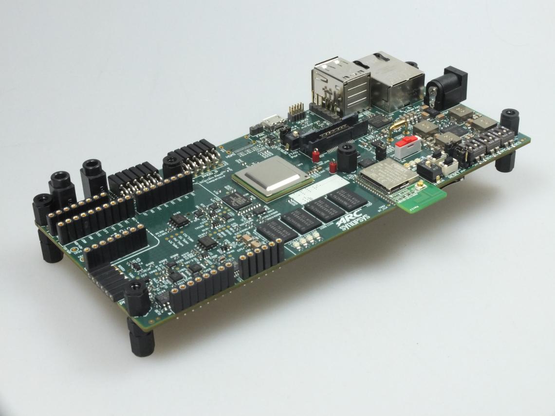
Bronco Webinar 800x100 1

Enhancing FPGA Prototype Debug

Enhancing FPGA Prototype Debug
by Daniel Nenni on 12-06-2017 at 7:00 am

FPGA prototyping is very popular in modeling hardware for early system prove-out, early embedded software development, as a cost-effective and performance-effective platform for software-driven hardware debug and for late-stage software debug, all before silicon is available. It has significant advantages in run-time performance over other hardware simulation methods and can be considerably less expensive than emulation. But as always, every solution comes with its own challenges; one particular challenge for FPGA prototyping is visibility into hardware internals for debug.

When using prototyping for hardware debug, good debug access is obviously critical; you have to be able to place probes / triggers wherever needed and you must be able to store long traces to debug back through sequences that may run for millions of cycles. In simulation-based verification this is easy. Changing observation points and triggers is simple and re-running after making a change to the design is equally simple.

But in FPGA prototyping neither of these steps is so easy. Take first the debug capability. Standard FPGAs, typically from Xilinx or Intel/Altera provide debug support in the form of on-chip logic analyzers (LAs), but these offer limited and potentially expensive debug support. First, they use extra gates, routing and (on-board) memory, more of each being required the more you want to debug. Problems are particularly acute with memory. Storing traces over millions of clock cycles may burn up all your on-board memory, undermining your design needs.

This becomes even more complex when your design spreads across multiple FPGAs, as is common when prototyping designs of any reasonable size. Commercial prototyping systems support large designs by partitioning them across multiple FPGAs on a board, and potentially across multiple boards or even multiple enclosures. In cases like this, native device-based debuggers hit yet another problem. They are effective, as far as they go, in debug at a device level, but each device now represents just a part of your design. Moreover, multi-FPGA prototyping isn’t just about partitioning across FPGAs. Logic to pipeline signals through limited package pins and board-level logic to optimize communication between FPGAs, all artefacts of prototyping rather than features of your design, further complicate the debug picture from a whole design point of view.

There’s another problem (in case you though you could somehow work your way around the problems I have listed so far). Since probes are logic embedded in your design, if you need to change probes (which you will, given a very limited budget for debug logic when using LAs), you’ll need to re-implement the whole design on almost all debug iterations (because you’ll almost certainly need to add more probes). And that is going to take a lot of time per iteration – adding the probes to the RTL, resynthesizing, perhaps re-partitioning and re-implementing through FPGA place and route. Think days at least to add a few probes.

This is where dedicated debug solutions become particularly important, by moving most of the debug functionality off the FPGA so that the bulk of device resources remain allocated to your design, by supporting many more probes per device than would be possible in LAs and by letting you interact with a view of your total design (which is what you really want to understand) by transparently handling the details of design to device mapping. I’ll illustrate this through the S2C MDM (multi-debug module) solution.

On resources, consider first memory needs. MDM doesn’t use FPGA memory. All debug data is output through a DDR3 memory port to external memory on the MDM board. Freed of the highly constrained FPGA memory resources, the solution provides 16GB of memory, supporting up to 16K probes per FPGA and several million cycles of traces. The on-device support logic is also greatly reduced to the very limited circuity, even for 16K probes, needed to capture and stream out this data.

This also largely addresses the design iteration (for debug) problem. With 16K probes per FPGA, you’ll need a lot less lengthy design rebuilds to complete debug. Which means that getting to verification closure is going to be a lot faster.

Finally, the MDM solution works with up to 16 FPGAs simultaneously. And through the Prodigy Player Pro cockpit, you can interact with your design in selecting probes, viewing waveforms and tracing back to find root-causes, all without having to worry about the mapping details between the design and the FPGA implementation. Together this provide a debug solution much closer to what you are used to in simulation.

You can learn more about the S2C Multi-Debug Module HERE.


Jump Start your Secure IoT Design with Intrinsix

Jump Start your Secure IoT Design with Intrinsix
by Mitch Heins on 12-05-2017 at 12:00 pm

Have you ever had a great idea for a new product but then stopped short of following through on it because of the complexities involved to implement it? It’s frustrating to say the least. It is especially frustrating, when the crux of your idea is simple, but complexity arises from required components that don’t add to the functionality of the design. Enter the world of an internet-of-things (IoT) device.

By definition, IoT devices live in the “wilds” of the internet, and that means they need to be made secure, else we endanger not only our own application but the internet upon which it depends. In most cases, IoT devices are made up of a simple processing unit, a network interface, and one or more sensors/actuators. These devices are typically much simpler than the required security element. This begs the question of how to bridge the security gap without having to hire an entire security team to design a secure device.

Depending on your device there are multiple options. Some CPU vendors have a complete and comprehensive approach to security built into their offerings. These offerings typically require some type of licensed IP. Alternately, some operating systems like Linux, can also provide for secure communications. Security algorithms are implemented in software and as such require sophisticated CPUs to implement them. However, many IoT devices don’t need or want the more powerful CPUs. In fact, the opposite is true. They need just enough computing power to talk to their sensors/actuators and then relay the information on to an IoT gateway. These devices need to be very low power, running on the smallest of batteries, while also being extremely cost sensitive.

Intrinsix, a leading design services company, addresses the IoT security gap by providing a Secure IoT Jump-Start kit. The kit enables designers to quickly realize IoT designs with the required performance and security while using a minimized design architecture that is frugal on power. The Jump-Start kit makes use of a RISC-V processor which can be easily configured to use minimal features and this cuts down on both chip size, power and cost.

Security is provided through a custom IoT security hardware accelerator IP that dramatically reduces power consumption by as much as 1000X and increases battery life by as much as 10X. This frees up the CPU to be further customized for the specific application. The security IP is certified to be NSA Suite-B compliant (meeting NSA Secret level requirements), more than sufficient for most IoT applications.

The Jump-Start kit also makes use of the minimalist Zephyr OS which does away with the need for more sophisticated memory management needed by operating systems like Linux. This means you don’t need to have a dedicated MMU, further reducing the chip footprint and cost.

To make system design easier Intrinsix also includes within the Jump-Start kit a full software stack and API to access the dedicated security hardware accelerator. The software comes with example code that developers can use as a guide for linking security into all transactions into and out of the device. Of course, being a design services company, Intrinsix can be called upon to help implement a portion or all of the system for their customers.

In summary, the Intrinsix IoT Jump-Start kit is meant to give IoT system designers a way to jump over the IoT security gap and to enable them to get their initial IoT product up and running and into the market with a secure system while reducing risks and both non-recurring and recurring costs.

You can learn more about Intrinsix and their IoT offerings online at the link below or by downloading their IoT e-book.

See also:
Intrinsix eBook: IoT Security The 4[SUP]th[/SUP] Element
Intrinsix website


Blurring Boundaries

Blurring Boundaries
by Bernard Murphy on 12-05-2017 at 7:00 am

I think most of us have come to terms with the need for multiple verification platforms, from virtual prototyping, through static and formal verification, to simulation, emulation and FPGA-based prototyping. The verification problem space is simply too big, in size certainly but also in dynamic range, to be effectively addressed by just one or even a couple of platforms. We need microscopes, magnifying glasses and telescopes to fully inspect this range.


Which is all very well, but real problems don’t neatly divide themselves into domains that can be fully managed within one platform. When debugging such a problem, sometimes you need the telescope and sometimes the microscope or magnifying glass.

This in turn means you need to be able to flip back and forth easily between these platforms. I wrote in an earlier blog (Aspirational Congruence) on a Cadence goal to make these transitions as easy as possible between emulation (on Palladium) and prototyping (on Protium). It looks like they have succeeded, so much so that the boundaries between emulation and prototyping are starting to blur. Frank Schirrmeister at Cadence pointed me to three customer presentations which illustrate collaborative verification between these platforms.

One, from Microsemi, illustrates needs in bringing up hardware and firmware more or less simultaneously for multi-processor RAID SoCs. Need to model with software and realistic traffic make hardware assist essential, but they also must span a range for detailed hardware debug and power and performance modeling to the faster performance required for regressions, where detailed debug access is not necessary. If a regression fails on the prototyper they may want to drop that case back onto the emulator, a step greatly simplified by the common compile front-end and memory backdoor access between the platforms.

Amlogic, who build over-the-top set-top boxes, media dongles and related products have similar needs but helpfully highlighted different aspects of the benefits of using a mixed prototyping/emulation flow. Their systems obviously depend on a lot of software (they have to be able to boot Linux and Android in full-system debug) and naturally some post-boot problems straddle both hardware and software. Again, they saw the benefit of speed in prototyping with ease of switching back to emulation for detailed debug. An interesting point here is that Amlogic used hands-free setup for Protium, which gave them 5MHz performance over 1MHz on Palladium. And probably a pretty speedy setup since they weren’t trying to tune the prototype; yet this apparently delivered enough performance for their needs. Amlogic’s measure of the effectiveness of this flow was pretty simple. They were able to get basic Android running on first silicon after 30 minutes and deliver a full Android demo to a customer in 3 days. That’s pretty compelling.

Finally, Sirius-XM Radio gave a presentation at DAC this year on their use and benefits in this coupled configuration. (If you weren’t aware, Sirius-XM designs all the baseband devices that go in every satellite receiver.) There are some similar needs, but also some interesting differences. Between satellites, ground-based repeaters and temporary loss of signal (going under a bridge for example), there’s significant interleaving of signals spanning between 4-20 seconds which must be modeled. Overall for their purposes they have to support 2 full real-time weeks of testing; both of these needs obviously require hardware assist. Historically they did this with their own custom-crafted FPGA prototype boards, but observed that this wouldn’t scale to newer designs. For example, for the DDR3 controller in their design, they had to use the Xilinx hard macro, which didn’t correspond to what they would build in silicon and might have (had they followed this path on their latest device) led to a silicon re-spin bug.

Instead they switched to a Palladium/Protium combo where they could model exactly what they were going to build. They used the Palladium for end-to-end hardware verification, running 1.5 minutes of real-time data in 15 hours. Meantime, the software team did their work on a Protium platform, running 1.5 minutes of real-time data in 3 hours, which served them well enough to port libraries, the OS and other components and to validate all of these. Again, where issues cropped up (which they did), the hardware team was able to switch the problem test-run over to the Palladium where they could debug the problem in detail.

The thread that runs through all these examples is default (and therefore fast) setup on the prototyper being good enough for all these teams, and ease of interoperability between the emulator and the prototyper. For hardware developers, this supports switching back from a software problem in prototyping to emulation when you suspect a hardware bug and need greater visibility. Equally, the hardware team could use the prototyper to get past lengthy boot and OS bring-up, to move onto where the interesting bugs start to appear. And for software developers, this setup enabled work on porting, development and regression testing using the same device model used in hardware development. For each of these customers, the bottom line was that they were able to bring up software on first silicon in no more than a few hours. Who wouldn’t want to be able to deliver that result?


35 Semiconductor IP Companies Hold 2nd Annual Conference

35 Semiconductor IP Companies Hold 2nd Annual Conference
by Daniel Payne on 12-04-2017 at 12:00 pm

Our smart phone driven semiconductor economy consumes a lot of IP blocks to enable quick product development cycles, often annually updating with new models to choose from. So where do you find all of the best semiconductor IP, verification IP and embedded software? Well, one place is at the 2nd annual REUSE conference, scheduled for December 14th in Santa Clara at the Convention Center where you’ll be able to explore what 35 companies have to offer. Here’s the list to pique your curiosity a bit:

  • arm
  • Achronix
  • Amphion
  • Andes Technology
  • Archband
  • Avery Design Systems
  • CAST
  • Certus Semiconductor
  • City Semiconductor
  • Corigine
  • efabless
  • flexlogix Technologies, Inc.
  • Intel
  • Intrinsic ID
  • menta
  • mixel
  • Mobile Semiconductor
  • mobiveil
  • Moortec
  • NSCore
  • nvm engines
  • Open Silicon
  • QuickLogic
  • Samsung
  • SiFive
  • Silicon Creations
  • Silvaco
  • SiNTEGRA
  • Sofics
  • Sonics
  • surecore
  • SmartFlow
  • Semi IP Systems
  • True Circuit Inc
  • Uniquify

It’s refreshing to see such a wide span of vendors at this conference, from small start-ups to behemoths like arm, Intel and Samsung. Even at the first annual REUSE conference last year there were some 34 companies from 11 countries signed up, and 400 attendees registered, pretty impressive for an inaugural event.

I contacted Warren Savage of Silvacoto find out more about REUSE because he was one of the founders of this new conference. Online Warren has been making YouTube videos for several years under the tagline of Take Five with Warren where he interviews key people in the semiconductor IP industry. Each video plays in about 5 to 7 minutes, so don’t get hung up on the literal 5 minute moniker.

Warren started out in 1979 as a design engineer at Fairchild Semiconductor, then moved into management with Tandem for 13 years. He started in the IP business with Synopsys from 1995 to 2003, then became President and CEO of IPextreme for the next 12 years. Last year in June his company IPextreme was acquired by Silvaco, where Warren is now the General Manager of the IP division.

Q&A

What type of engineer would be interested in attending?
Anyone that uses IP will probably find something interesting there. It’s a great venue to come and check out companies that you may not have had a chance to see at DAC or other shows, which are so much more expensive for nascent IP companies to attend.

What does an engineer get out of attending in terms of benefit, ideas, skills, awareness, etc?
As I mentioned, one of the principles is that we don’t have a committee that tells people what they can and cannot talk about. We let companies talk about anything they like, and usually they pick something that they think would be interesting to someone. Whether its applicable to a design engineer or a product manager, we don’t know. They can read the agenda and find something interesting, I’m sure.

Are there speakers at the event?

Yes, a really nice selection of IP companies, big and small. Plus some nice keynotes from Smartflow on IP piracy and from Samsung on what IP means to foundries. Plus, Intel is giving a talk on what they expect from IP suppliers.

  • Ted Miracco, CEO, SmartFlow Compliance Solutions
  • Heather Monigan Program Director & Technology Strategist, Intel
  • Hong Hao, Sr. VP Foundry Business, Samsung
  • Meredith Lucky, VP of Sales, CAST
  • Tony Kazaczuk, Director, Flex Logix
  • Warren Savage, GM, Silvaco
  • John Heinlein, Ph. D., VP, Arm
  • Timothy Saxe, Ph. D., VP and CTO, QuickLogic
  • Stephen Fairbanks, Co-Director, Certus Semiconductor
  • Brian Gardner, VP of Business Development, True Circuits, Inc.
  • Steve Mensor, VP of Marketing, Achronix Semiconductor
  • Mike Noonen, Silego Technology
  • Dr. Naveed Sherwani, President & CEO, SiFive
  • John Blyler, JB Systems
  • Michael, Wishart, CEO, efabless
  • Andrew Cole, VP, Silicon Creations
  • Jim Bruister, Director, Silvaco

What is happening in the IP industry these days?
I think that attendees can get a very good sense of the dynamics of the industry by attending, listening to the talks and visiting with suppliers and other attendees. My sense is that the IP industry is as strong as ever and we continues to morph into new areas.

Is the event expensive to attend?
No, it’s free this year to attend.

How many people do you expect this year?
I expect between 500-600 people this year.

Registration
Even though this conference is free, you must register online to reserve your spot and receive a lanyard at the event.

REUSE 2017will again bring the global IP community together, this time at the Santa Clara Convention Center in the center of Silicon Valley. Here an even greater diversity of suppliers will be promoting their products in a fair and balanced showcase. REUSE will also provide an open forum for communication and networking within our industry.


What are you ready to mobilize for FPGA debug?

What are you ready to mobilize for FPGA debug?
by Frederic Leens on 12-04-2017 at 7:00 am

There are 3 common misconceptions about debugging FPGA with the real hardware:

[LIST=1]

  • Debugging happens because the engineers are incompetent.
  • FPGA debugging on hardware ‘wastes’ resources.
  • A single methodology should solve ALL the problems.

    Continue reading “What are you ready to mobilize for FPGA debug?”


  • RISC-V Business

    RISC-V Business
    by Tom Simon on 12-04-2017 at 7:00 am

    I was at the 7[SUP]th[/SUP] RISC-V Workshop for two days this week. It was hosted by Western Digital at their headquarters in Milpitas. If you have not been following RISC-V, it is an open source Instruction Set Architecture (ISA) for processor design. The initiative started at Berkeley, and has been catching on like wildfire. There are a number of RTL implementations that work in FPGA’s or SOC’s and there is also production silicon from companies such as Si-Five. The RISC-V Workshop was sold out with over 500 attendees – most of whom stayed for the full two days.

    The agenda was filled with detailed technical presentations from a wide range of institutions and companies. They covered details of proposed additions to the specification, commercial products using RISC-V, and research projects leveraging the ISA. The presenters talked about everything from server farm simulation, machine learning, debugging tools, novel applications, and more.

    The keynote was given by Western Digital CTO Martin Fink. He had several surprising things to tell us. First off, after talking in depth about Western Digital’s take on big data versus fast data, he mentioned that Western Digital actually ships about 1 billion processors a year. These processors enable USB drives, hard drives, solid state drives and more. They play a crucial and growing role in moving and processing data. We are all familiar with the cache schemes to improve performance and monitoring to maintain data integrity. In the future, filtering and processing might even occur on the storage device directly, aided by more advanced and powerful processors.

    The second surprising announcement that Martin made was that Western Digital is committing to transition all of these processors to RISC-V. While unexpected, it probably should not have come as a complete surprise. The slide showing companies supporting RISC-V barely has any white space on it these days. Almost every large semiconductor company is represented.

    The two days of talks made clear that the RISC-V ecosystem is being built out at a rapid pace and there is a lot of momentum. Low end implementations of RISC-V were handed out to some of the guests in a smart name tag designed by Antmicro that uses the E310 from Si-Five. Si-Five has announced a 5-core chip that is suitable for running Linux. At the upper end of the performance spectrum, a new company called Esperanto came out of stealth mode at the Workshop to announce its technology that uses massively parallel RISC-V processor chips to tackle machine learning.

    I’ll be writing more about RISC-V, but because it is open source, you can go directly to the RISC-V website and view the specs and learn about the current implementations, development tools and future work planned to add to the spec. It’s worth noting that the core parts of the ISA are already defined and frozen, so they can be relied upon for development.

    RISC-V has the potential to be as transformative as Linux, or HTML. It appears to have the ability to scale from MCU to server class. Already people are using it in a wide range of applications. As an analyst, I attend a lot of technology events and I think the turnout and enthusiasm for this event was exceptional.


    IP-SoC 2017: IP Innovation, Foundries, Low Power and Security

    IP-SoC 2017: IP Innovation, Foundries, Low Power and Security
    by Eric Esteve on 12-03-2017 at 12:00 pm

    The 20[SUP]th[/SUP] IP-SoC conference will be held in Grenoble, France, on December 6-7, 2017. IP-SoC is not just a marketing fest, it’s the unique IP centric conference, with presentations reflecting the complete IP ecosystem: IP suppliers, foundries, industry trends and applications, with a focus on automotive. It will be also the celebration of Design & Reuse 20[SUP]th[/SUP] anniversary, and the conference program is very high level, with people like Aart De Geus, chairman and Co-CEO of Synopsys or Sir Robin Saxby, the founder of ARM, presenting keynotes to start the conference.

    You probably know Charles Janac, CEO, ArterisIP, the chairman of the session “The Past and the Next Decade Vision”. If you remember, he was CEO of Arteris when the company was acquired by Qualcomm in 2013 for several hundred million dollars… but, in fact, only the Network-on-Chip (NoC) IP portfolio was acquired and Arteris became ArterisIP, still developing and selling NoC IP.

    In this session, Mark Ma will give a review of China IP to IC industry in 2017, Eklovya Sharma (Sankalp Semiconductor) will tell how he expects “Changing dynamics in semiconductor industry” and Bill finch from Cast will share his experience about the “Reusable IP Revolution and How a Small Company Took Advantage”… Last year, Bill Finch has given a presentation at IP-SoC “Back to the Future. The End of IoT”, and I admit that it was provocative, but I loved it! The presentation summary was: The term Internet of Things is the most over used, over hyped, mis-used and mis-understood phrase of the last few years. It now has so many meanings that it has become useless to describe anything worthwhile. As designers of IP and electronic systems we need to refocus on what we want to accomplish going forward. As always, it’s about customer needs and long term benefits. I will certainly attend to Bill’s presentation this year.

    If a business need an ecosystem to grow and develop, this is certainly the IP business. And foundries are with EDA a very strategic part of this ecosystem. That’s why the “Foundry Vision” session is dedicated to IP friends like Samsung, GlobalFoundries and Soitec. There is a clear focus about FDSOI technology, as a reminder, Soitec is the #1 SOI wafer provider and GF will talk about FDXcellerator and 22FDX ecosystem. Don’t expect me to complain about this FDSOI focus as I have written numerous blogs, along with other at Semiwiki like Paul Mc Lellan, to introduce FDSOI technology to our readers in 2012-2013, even before the technology being adopted by Samsung and GlobalFoundry as a mainstream solution, complementary with more power-hungry FinFET technology. In FDSOI we trust, especially for battery powered applications, in pure digital or RF IC!

    There will be other sessions dealing with IP ecosystem, like “From IP to SoC: What is the Trend” or “Automotive IP and Software”. You will hear about Analog IP from Mahesh Tirupatur with Analog Bits, one of the most talented IP vendor dealing with highly complex IP, from engineering standpoint, or Interconnect IP from Charles Janac (ArterisIP). Embedded FPGA will be honored by no less than two vendors, Flex Logix Technologies and Menta as Imen Baili (Menta) will explain why “eFPGA is the key solution for Automotive embedded systems”.

    You should stay up to Thursday 7[SUP]th[/SUP] , as the 2[SUP]nd[/SUP] day is very busy with very interesting topics, in these seven sessions:

    – –Power Management and IoT vision (Microchip, Synopsys and CSEM)

    – –Security (Inside Secure, Dolphin Integration and Secure IC)

    – –Design methodology, Innovative IP in FD-SOI Technology, IP SoC design and System design

    IP-SoC 2017 is clearly this kind of high level conference where complexes engineering topics are addressed by industry experts, not just a marketing fest!

    IP-SoC conference will be located on December 6-7 in Hôtel EUROPOLE, 29 rue Pierre-Sémard, Grenoble Grenoble, France, you can register here

    See you on Wednesday 6[SUP]th[/SUP] December in Grenoble

    From Eric Esteve from IPNEST


    Making Your Next Chip Self-Aware

    Making Your Next Chip Self-Aware
    by Daniel Payne on 12-01-2017 at 12:00 pm

    One holy grail of AI software developers is to create a system that is self-aware, or sentient. A less lofty goal than sentient AI is for chip designers to know how each specific chip responds to Process variations, Voltage levels and Temperature changes. If a design engineer knew exactly which process corner that each chip was fabricated under, then they could dynamically control each chip to perform in an optimal manner. If I knew how much current my transistors consumed with a simple test measurement, then I could predict which test bin they should fall into instead of running a complete functional test. If I could measure the performance of my transistors over time, then I could predict their performance during the aging process and make adjustments to the operating conditions. The list of benefits is quite long if only there was a method to measure the PVT characteristics of each chip.

    Crafty engineers have figured out how to enable these benefits through something called embedded in-chip monitoring, placing special circuits onto each chip that can dynamically measure and report process variation, voltage levels and temperature values. Moortec is such a company that has commercialized on-chip monitoring and offering the SoC industry their IP application, integration and device test during production since 2005, based in Plymouth, UK.


    Here are some reasons that you should consider adding embedded in-chip monitoring:

    • Measure process variation per chip
    • Dynamically measure voltage levels for VDD during chip operation
    • Enable Dynamic Voltage and Frequency Scaling (DVFS) to control power consumption
    • Support Adaptive Voltage Scaling (AVS) to manage power
    • Optimize your CMOS designs from 40nm down to 7nm process nodes

    As device geometries get smaller the variations in switching speed delays start to increase as a function of supply voltage, so knowing your internal VDD levels is critical to performance.


    Switching speed delay variations against supply voltage for a number of different process technologies

    Voltage threshold values shift over time caused by negative bias temperature instability (NBTI) and hot carrier injection (HCI), so being able to measure your Vt values over time is crucial for reliable operation.


    V degradation due to NBTI and HCI

    To learn more about embedded in-chip monitors from the experts at Moortec then you should consider attending their upcoming webinar online.

    Webinar Details

    Who Should Attend?
    The webinar is aimed at IC developers and engineers working on advanced node CMOS technologies from 40nm down to 7nm, will also highlight the challenges posed by process, temperature and voltage variability and how those challenges relate to the stability of complex SoC designs. Moortec provide complete PVT Monitoring Subsystem IP solutions on 40nm, 28nm, FinFET and 7nm. As advanced technology design is posing new challenges to the IC design community, Moortec are able to help our customers understand more about the dynamic and static conditions on chip in order to optimize device performance and increase reliability. Being the only PVT dedicated IP vendor, Moortec is now considered a centre-point for such expertise.

    About Moortec
    Established in 2005, Moortec provide in-chip monitors and sensors, such as embedded Process Monitors (P), Voltage Monitors (V) and Temperature Sensors (T). Moortec’s PVT monitoring IP products enhance the performance and reliability of today’s Integrated Circuit (silicon chip) designs. Having a track record of delivery to tier-1 semiconductor and product companies, Moortec provide a quick and efficient path to market for customer products and innovations. For more information please visit www.moortec.com


    Hierarchy Applied to Semiconductor IP Reuse

    Hierarchy Applied to Semiconductor IP Reuse
    by Daniel Payne on 11-30-2017 at 12:00 pm

    When I first started doing IC design back in 1978 we had hierarchical designs, and that was doing a relatively simple 16Kb DRAM chip with only 32,000 transistors using 6um (aka 6,000 nm) design rules. SoC designs today make massive use of hierarchy at all levels of IC design: IC Layout, transistor netlist, gate level netlist, RTL level, C or SystemC level, embedded software, software drivers, firmware. Our semiconductor IC business is based on both IP and EDA tools being able to handle hierarchy effectively.

    One company in the EDA space that knows quite a bit about IP reuse is Methodics, because they’ve built a company that focuses on IP use and reuse. Their latest generation IP management system is a software tool called Percipient that enables IP reuse for a wide range of IC design teams where a user and manage their IP as a collection of dependent, hierarchical building blocks, then reuse entire hierarchies instead of single IP blocks.

    The methodology in using Percipient is that everything in the design hierarchy is treated as IP, starting at the top-level of the SoC, down to a module, a block, even a cell like a PLL. So your project in Percipient can be at any level of hierarchical description, enabling elegant reuse. In the following diagram we can see a USB Controller that has a regular resource of a USB PHY cell along with a private resource of a USB TestBench:

    The USB TestBench is a private resource that makes sense to use when the USB controller is used in a standalone context, but not while actually using the IP as part of a larger design. At the top-level of my SoC I don’t really need to carry around this private resource of a USB TestBench. As I place this USB Controller into an IO Subsystem the private resources are noted, and these private resources are visible only to a certain level of the IP, but not the parent IP.

    The IO TestBench is relevant to the IO Subsystem only, but as I place this IO Subsystem into my SoC as another IP block then I don’t need to see or deal with the lower-level private resources any longer. So I can use this IO Subsystem multiple times on different projects and not be concerned with the private resources associated with it.

    So, what do we get with a context-dependent resource (aka Private Resource)?

    • Manage peripheral resources (stimulus generators, testbenches, PDKs, etc) as IPs in my system for tracking, releases, or caching.
    • Reuse any IP easily in a variety of contexts while not having to make any context-specific changes.
    • Customize my development environment of IP blocks while not interfering with private resources in their separate context.

    Hierarchy is a wonderful thing and is commonly used within EDA tool flows, so its refreshing to know that Methodics has figured out how to support hierarchy as part of the larger IP management task by supporting the concept of private resources, allowing us to manage these private resources along with all of our other IP. At the top-level of my SoC I can see just the IP blocks that I need to manage my project, and I don’t need to be bothered with lower-level IP blocks that only pertain to a different context. With Percipient I just see what I need to at each level of the hierarchy.

    White Paper
    To get more insight into this topic then read the four page White Paper at the Methodics web site here.

    Related Blogs

    ISO 26262 for Semiconductors
    The attractive automotive market has some unique safety requirements that are defined in the ISO 26262 standard. To learn more about how design data and IP lifecycle management fits into the ISO 26262 standard then consider attending the roundtable discussion led by Methodics at the December 6th event in Munich, Germany.


    A Crossover MCU

    A Crossover MCU
    by Bernard Murphy on 11-30-2017 at 7:00 am

    Back in the day we had processors which consolidated computing power onto a chip, and out of these sprang (if you’ll excuse the Biblical imagery) microcontrollers (MCUs) in one direction and increasingly complex system-on-chip (SoC) processors in another direction. SoCs are used everywhere today, in smartphones, many IoT devices, networking switches and many more applications. MCUs played a vital though less glamorous role in machine control, handling our anti-lock braking (ABS) and fuel-injection, in implanted medical devices, power tools and many other applications your probably never realized contained a processor.


    A key characteristic of these systems was absolute reliability and real-time responsiveness. You probably don’t care about hooking up your pacemaker or your ABS to iTunes, but you very much do care that they will work dependably (no need to reboot constantly) and will continue to do so for many years. So the great majority of development in MCUs went into cost, low power, reliability and support for RTOS, while functional advances moved more slowly.

    But IoT pressures have changed this landscape. Now there is a greater need for future-proofing as communication, security and other standards evolve. System builders expect to be able to gather data from these systems to process in the cloud, they expect to be able to support over-the-air (OTA) updates to minimize maintenance costs and keep systems relevant and compliant, they need to support higher levels of performance and they need support for the aggressive types of power management used today in applications processors (APs).

    All of this while, of course, still providing the reliability and real-time response for which MCUs are known. You can’t just replace all the MCUs with APs. APs don’t provide RTOS–grade support since they have (among other things) unpredictable interrupt latencies. But you still want all those goodies you get in an AP. Getting to this is a big deal. I think I’m remembering an ARM-provided statistic correctly when I say that ~80% of the systems built on their platforms are MCUs, so these are huge volumes waiting for these devices if this transition is possible.

    Taking a leaf from the automakers playbook, NXP (who are very well known in this market) have chosen to address this need though what they call a crossover MCU. This is quite a device (actually a small family of devices – iMX.RT). It’s based on a Cortex-M7, supporting RTOS operation and delivering, apparently, 50% higher performance than similar products. It provides 2-D graphics support, camera interface, LCD controller and hi-performance audio support. And it provides interfaces to wireless connectivity for WiFi, Bluetooth, BLE, ZigBee and Thread. Remember – this is an MCU.

    It provides a wide range of memory interfaces and on-board supports for AES, High-Assurance Boot and on-the-fly flash decryption. And the device includes an integrated PMIC so you can manage power directly without need for an extra device on your board. You can naturally leverage the NXP and ARM development ecosystems, there are dev boards, and so on.

    NXP told me that this MCU is already available in TSMC 40nm and 28nm FDSOI with Samsung, which they believe provides a good roadmap towards RF and non-volatile additions to the family. And of course they’re working on shrinks and lower node implementations. Sounds to me like these crossover devices may be the wave of the future in advanced MCU applications. And potentially even in less advanced applications if we expect to wire them into the IoT. Maybe not my toothbrush though. You can read more about these processors HERE.