The Internet of things (IoT) is growing rapidly and 2018 will be a fascinating year for the IoT industry. IoT technology continues to evolve at an incredibly rapid pace. Consumers and businesses alike are anticipating the next big innovation. They are all set to embrace the ground-breaking impact of the Internet of Things on our lives like ATMs that report crimes around them, forks that tell you if you are eating fast, or IP address for each organ of your body for doctors to connect and check.
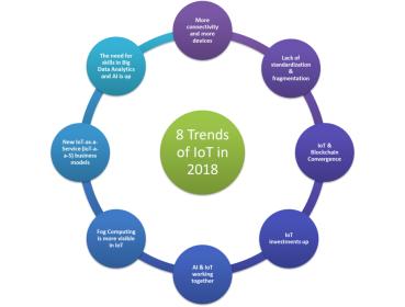
In 2018, IoT will see tremendous growth in all directions; the following 8 trends are the main developments we predict for next year:
Trend 1 —Lack of standardization will continue
Digitally connected devices are fast becoming an essential part of our everyday lives. Although the adoption of IoT will be large, it will most likely be slow. The primary reason for this is lack of standardization.
Though industry leaders are trying to develop specified standards and get rid of fragmentation, it will still exist. There will be no clear standards in the near future of IoT. Unless a well-respected organization like IEEE stepped-in and leads the way or the government imposes restrictions on doing business with companies if they are not using unified standards [6].
The hurdles facing IoT standardization can be divided into 3 categories; Platform, Connectivity, and Applications:
- Platform: This part includes the form and design of the products (UI/UX), analytics tools used to deal with the massive data streaming from all products in a secure way, and scalability.
- Connectivity: This phase includes all parts of the consumer’s day and night routine, from using wearables, smart cars, smart homes, and in the big scheme, smart cities. From the business perspective, we have connectivity using IIoT (Industrial Internet of Things) where M2M communications dominating the field.
- Applications: In this category, there are three functions needed to have killer applications: control “things”, collect “data”, and analyze “data”. IoT needs killer applications to drive the business model using a unified platform.
All three categories are inter-related, you need all them to make all them work. Missing one will break that model and stall the standardization process. A lot of work needed in this process, and many companies are involved in each of one of the categories, bringing them to the table to agree on a unifying standards will be a daunting task [12].
Trend 2 — More connectivity and more devices
The speedy proliferation of IoT in past 3 years has resulted in billions of interconnected devices. As the consumer continues to stay hooked to more gadgets. The number of connected devices grew exponentially every year. By 2018 it will at least double and touch a whopping the mark of 46 Billion by 2021. More IoT devices will enter the channels, more than ever before. A clear indication of our direct dependency over the gadgets and that’s how our future is shaped.[6]
As IoT continues to expand we will certainly see an increase in devices connected to the network in different areas in business and consumer markets. Smart devices will become the de-facto for people to manage IoT devices. The benefits of using smart devices in that capacity include boosting customer engagement, increasing visibility, and streamlining communication that will include new human-machine interfaces such as voice user interface (VUI) or Chatbot.[4][2]
Trend 3 — “New Hope” for security: IoT & Blockchain Convergence
As with most technology, security will be the major challenge that needs to be addressed. As the world becomes increasingly high-tech, devices are easily targeted by cyber-criminals. Evans Data states that 92% of IoT developers say that security will continue to be an issue in the future. Consumers not only have to worry about smartphones, other devices such as baby monitors, cars with Wi-Fi, wearables and medical devices can be breached. Security undoubtedly is a major concern, and vulnerabilities need to be addressed.
Blockchain is a “new hope” for IoT Security. The astounding conquest of Cryptocurrency, which is built on Blockchain technology, has put the technology as the flag bearer of seamless transactions, thereby reducing costs and doing away with the need to trust a centered data source.
Blockchain works by enhancing trustful engagements in a secured, accelerated and transparent pattern of transactions. The real time data from an IoT channel can be utilized in such transactions while preserving the privacy of all parties involved.[4][2]
The big advantage of blockchain is that it’s public. Everyone participating can see the blocks and the transactions stored in them. This doesn’t mean everyone can see the actual contents of your transaction, however; that’s protected by your private key.
A blockchain is decentralized, so there is no single authority that can approve the transactions or set specific rules to have transactions accepted. That means there’s a huge amount of trust involved since all the participants in the network have to reach a consensus to accept transactions.
Most importantly, it’s secure. The database can only be extended and previous records cannot be changed (at least, there’s a very high cost if someone wants to alter previous records). [10][3][4] [7]
In 2018 increased interest in Blockchain technology will make the convergence of Blockchain and IoT devices and services the next logical step for manufacturers and vendors, and many will compete for labels like “Blockchain Certified”.
Trend 4 — IoT investments will continue
IDC predict that spending on IoT will reach nearly $1.4 trillion in 2021. This coincides with companies continuing to invest in IoT hardware, software, services, and connectivity. Almost every industry will be affected by IoT, which means many companies will benefit from its rapid growth. The largest spending category until 2021 will be hardware especially modules and sensors, but is expected to be overtaken by the faster growing services category. Software spending will be similarly dominated by applications software including mobile apps.
IoT’s undeniable impact has and will continue to lure more startup venture capitalists towards highly innovative projects. It is one of those few markets that have the interest of the emerging as well as traditional venture capital. While the growth next year is firmly attested and the true potential is yet to be unearthed, IoT ventures will be preferred over everybody else. Many businesses have assured adding IoT to their services model from the Transportation, Retail, Insurance and Mining industries [4][6].
Trend 5 — Fog Computing will be more visible
Fog computing allows computing, decision-making and action-taking to happen via IoT devices and only pushes relevant data to the cloud, Cisco coined the term “Fog computing “and gave a brilliant definition for Fog Computing: “The fog extends the cloud to be closer to the things that produce and act on IoT data. These devices, called fog nodes, can be deployed anywhere with a network connection: on a factory floor, on top of a power pole, alongside a railway track, in a vehicle, or on an oil rig. Any device with computing, storage,andnetwork connectivity can be a fog node. Examples include industrial controllers, switches, routers, embedded servers, and video surveillance cameras.”
The benefits of using Fog Computing are very attractive to IoT solution providers, some of these benefits: minimize latency, conserve network bandwidth and operate reliably with quick decisions. Collect and secure wide range of data, move data to the best place for processing with better analysis and insights of local data. Blockchain can be implemented at the level of fog nodes too. [11]
Trend 6 — AI & IoT will work closely
Amalgamation of IoT data analytics with AI for applications ranging from elevator maintenance to smart homes, will progress rapidly over the coming two years. Platform and service providers are increasingly delivering solutions with integrated analytics designed to feed data directly into AI algorithms. Another important advantage of using AI is supporting the optimization and adaptation of both IoT devices and related processes and infrastructure.
AI can help IoT Data Analysis in the following areas: data preparation, data discovery, visualization of streaming data, time series accuracy of data, predictive and advanced analytics, and real-time geospatial and location (logistical data). [10]
Trend 7 — New IoT-as-a-Service (IoT-a-a-S) business models
Transformational business models will develop in many IoT verticals over 2018-2019, supported by Big Data and AI tools. In these models, the value is in the convenience of the service for end customers (on-demand and not requiring heavy upfront expenditure), and the usage data that is collected, analyzed, and fed back into suppliers’ businesses and processes.
But the potential for IoT business model transformation extends beyond this, to encompass an increasing variety of more complex, as-a-service business models that disrupt existing industries, particularly for areas such as heavy industry, transport and logistics, and smart cities.
For these industries, IoT solutions can enable more of an ongoing, managed service relationship with both technology providers and end customers. One selling point is that costs can be more directly linked to ongoing measured usage or to specific trigger events captured by IoT sensors (e.g., “break-the-glass” solutions in which sensors pick up when a building or car is broken into). Another is that costs may be spread over time, shifting from upfront Capex to a more regular Opex outflow. Examples of such models include lighting-as-a-service (L-a-a-S), rail-as-a-service (R-a-a-S), and even elevators-as-a-service (E-a-a-S).[1]
Trend 8— The need for skills in IoT’s Big Data Analytics and AI will increase
Dynamic data sharing is at heart of IoT and Big Data Analytics will be instrumental in building responsive applications. Integrating IoT data channels with AI to retrieve on demand analytical insights has already gained momentum this year and will definitely grow exponentially in 2018. Subsequently, the need for Big Data and AI skills will rise, while most IoT service providers have highlighted the shortage for such extensively skilled candidates, internal learning programs in close proximity with R&D has set to be launched in many companies.[1][10][8]
This article was published on IEEE-IoT
Ahmed Banafa Named No. 1 Top VoiceTo Follow in Tech by LinkedIn in 2016
Read more articles at IoT Trends by Ahmed Banafa
References:
[LIST=1]
http://www.ioti.com/strategy/five-internet-things-trends-watch
https://mobidev.biz/blog/iot-trends-for-business-2018-and-beyond
https://www.bayshorenetworks.com/blog/breaking-down-idc-top-10-iot-predictions-for-2017
https://readwrite.com/2017/10/03/6-iot-trends-2018/
https://lightingarena.com/internet-things-anticipated-trends-2018/
https://medium.com/@Unfoldlabs/seven-trends-in-iot-that-will-define-2018-2a47e763731c
https://datafloq.com/read/iot-and-blockchain-challenges-and-risks/3797
https://www.bbvaopenmind.com/en/five-challenges-to-iot-analytics-success/
https://www.bbvaopenmind.com/en/why-iot-needs-ai/
https://www.technologyreview.com/s/603298/a-secure-model-of-iot-with-blockchain/
https://datafloq.com/read/fog-computing-vital-successful-internet-of-things/1166
https://iot.ieee.org/newsletter/july-2016/iot-standardization-and-implementation-challenges.html
All figures: Ahmed Banafa
Also read:CEVA Ups the Ante for Edge-Based AI


