Software configuration management (SCM) has been around for a long time with commercial SCM offerings such as ClearCase and Perforce and public domain mainstays such as CVS and Subversion. Similarly, over the last two decades we’ve seen a big uptake in the adoption of hardware configuration management (HCM) methodologies driven by the exponential growth in systems-on-a-chip (SoCs) complexity, larger amounts of binary design data, an increased need for better control over data security, and the use of larger geographically-dispersed design teams.
More recently, the complexity growth is being exacerbated by newer heterogeneous SoC architectures required by the internet-of-things (IoT) devices. These devices fuse data from multiple different sensors and some even employ artificial intelligence techniques that combine both hardware and embedded software to process data before sending actionable information back to the cloud.
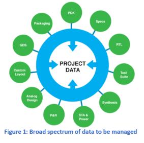
Managing SoC design data is particularly challenging when one considers that the design data is a composite of many different CAD abstractions and views. Design teams regularly use CAD tools from multiple electronic design automation (EDA) vendors, each which have their own data representations with different and many times incompatible databases. Layer on this the fact that designs also use multiple IP libraries, some built internally while others are from outside vendors.
Add to this the fact that design teams are comprised of engineers with varied backgrounds who are working on different steps of the design process, on different networks and different hardware platforms while geographically dispersed across the globe. These engineers have different responsibilities and access rights to project data that must be strictly enforced.
For any SoC design, it is necessary to effectively manage the sharing of completed design data while isolating data that is still in progress (e.g. shared libraries vs scratch libraries). Hardware teams have traditionally relied on human-based data gate-keeping to ensure engineers don’t inadvertently overwrite each other’s work when copying changes from scratch areas to master libraries. It’s a practice that is fraught with error and almost unmanageable for teams that cross multiple time zones.
Teams have tried to mitigate the time zone problem using multiple master libraries, which they try to keep in sync on a regular basis. The use of hierarchical design complicates this practice as changes to lower level cells may not be seen due to latency between updates to the different master libraries and the lack of a clean bill of materials detailing cell versions to be used by the project. A much bigger problem occurs when changes are not detected and the project tapes out. This sort of error can necessitate a very expensive re-spin. File management is also cumbersome in this arrangement with multiple copies being kept on each site for both use and archival, which increases the cost of the associated storage devices.
The biggest issue aside from the logistical management of files and databases is the lack of a common process for managing the numerous revisions on all views of the design. This is where a hardware configuration management tool comes in. Many companies have taken different approaches to resolving the issues unique to the hardware designer. While some have opted to build layers on top of existing SCMs such as subversion, others have taken the route of creating the HCM from the ground up, providing a better platform which can be easily customized to the different needs of hardware design teams.
SOS7, a HCM from ClioSoft, is a good example. ClioSoft’s SOS7 streamlines the design process and significantly improves a team’s productivity. It acts as a gatekeeper and protects the users from accidentally losing or overwriting valuable data, eliminating the need for manual bookkeeping. SOS7 employs a distributed Client-Server architecture that allows access to data irrespective of a user’s location. Data is stored once in a common project repository and the system makes use of remote cache servers to reduce network bandwidth and minimize the effects of network latency.
Most importantly, SOS7 ensures that design changes are seen immediately by all other members of the team, regardless of the hardware platform used, as SOS7 works cross platform and is available on both the Linux and Windows. SOS7 also provides for sandbox development areas to isolate changing data. Objects checked out for edit have write-locks to prevent accidental overwrites by others with the ability to revert to or view previous versions.
Especially important for safety critical applications requiring ISO 26262 certification is that SOS7 maintains audit trails of all changes made to the design. SOS7 also employs gate keeping policies for data access control and integrates data management with requirements and issue tracking systems such as Jira, Bugzilla and Trac.
While SCM systems deal with source code in the form of ASCII text files, HCM systems must deal with data in different EDA formats. EDA tools create many different types of side files used to manage their own data. Knowing which of these files to archive can be cumbersome, but SOS7 takes care of that automatically, making it easier to add or exchange tools within the design flow as needed. This is enabled by the EDA vendors providing application programming interface (API) support that allows SOS7 to manage their data for them. DM APIs enable the design flow to seamlessly support revision control with automatic check-out and check-in capabilities without requiring the designer to know all the nuances of which EDA files need to be stored and which can be ignored.
It is easy to do a diff with text files, but it is a different problem when it comes to binary files such as schematics or layout views. SOS7 can easily do the text diff capabilities like SCM, but it also goes the extra mile by providing a mechanism to highlight differences between versions of a schematic or layout. In addition, ClioSoft also added design management GUIs directly into the EDA tool library browsers and design editors to give engineers the capability to browse libraries and design hierarchies, examine the status of cells and perform revision control operations without leaving the design environment or learning a new interface.
For most SoC design teams, given the large amount of design data generated, and the increased number of globally dispersed designers, disk space storage remains a major concern. A HCM such as SOS7 works hard to ensure that the size of the repository remains as small as possible. It achieves this objective by intelligently using the notion of symbolic links to optimize disk space usage for static libraries and design files. All the design files in the designer’s workspace remain as read-only symbolic links which minimizes the disk usage considerably. It is only when the designer wants to edit the file that a writable view of the design file is made available in the workspace.
The take away from all of this is that with the advent of more complex SoCs being designed for IoT applications, hardware configuration management will no longer just be for the big enterprises. Even small teams will need to embrace HCM, not only for design complexity, but for the capability to be able to do safety critical designs that require an audit trail and good version control. And remember if you are a startup, you likely will be hoping to be acquired for your IP. Being able to show that your design process and data are clean and in control can make all the difference to an acquiring company as to whether your IP is considered valuable or a pile bones that only a few people can make work.
This all bodes well for ClioSoft and their DM solutions and I expect we will be hearing more from them as the IoT revolution continues to explode.
See also:
ClioSoft Products Overview
ClioSoft SOS – Virtuoso
ClioSoft Visual Design Diff