This year the Advanced Lithography Conference felt very different to me than the last couple of years. I think it was Chris Mack who proclaimed it the year of Stochastics. EUV has dominated the conference for the last several years but in the past the conversation has been mostly centered on the systems, system power and uptime.
I will be writing up more detailed blogs from interviews with ASML and imec and their presentations, but I wanted to first present some overall impressions.
ASML is now delivering systems with acceptable power (at least for initial use) and uptime is improving, although not there yet.
The conversation about EUV has now shifted into the practical details of the process parameters and there are lots of details to work through!
Perhaps the key issues remaining with EUV relates to dose and line edge roughness (LER). Dose is the number of photons delivered multiplied by the photon energy. because EUV photons are so much more energetic than deep UV (DUV) photons there are 18 times less photons in EUV for the same dose. The small number of photons leads to shot noise at low doses, but this is just the tip of the iceberg.
The random defects from EUV exposure can lead to micro bridges and open lines for line/space pairs and missing or bridged contacts in dense contact arrays. In his Keynote address Yan Borodovsky noted that complex designs can have up to one billion vias and a single bad via can kill the circuit. Under this condition even a five-sigma process will result in zero yield!
At Litho Vision held the Sunday before SPIE, John Biafore of KLA Tencor noted that current EUV photoresists only absorb about 20% of the incident EUV photons. Ideally a photoresist should absorb around 45% of the photons to maximize sensitivity while insuring even exposure down through the depth of the photoresist. This presents an opportunity to double the sensitivity of the photoresist doubling the effective dose for a given delivered dose. Of course, if this was easy it would already be done. The photoresist needs to absorb EUV photons and generate secondary electrons with the correct characteristics that trigger photo events.
In Patrick Naulleau’s talk “The implications of shot noise on EUV patterning” he made several interesting observations:
LER goes up exponentially at lower does and even at high dose it is never zero with around 1.5nm as a minimum.
For chemically amplified photoresists there are five reaction variables that determine LER:
[LIST=1]
The relative importance of the different mechanisms for a 16nm feature on line width roughness (LWR) are:
- Photon noise = 2nm
- Acid generation = 1.2nm
- PAG = 0.6nm
- Quencher = 1.9nm
- Protecting groups =0.1nm
The interesting conclusion for this is material related effects are more important than simple photon shot noise!
There continues to be a lot of work down on post exposure smoothing of photoresist and while there are promising results for specific features the broad applicability still need works.
Self-aligned blocks (SAB) and fully self-aligned (FSAV) are another interesting area that could in theory reduce sensitivity to LER/LWR but again the ability to broadly create all the required features needs work.
In “EUV photolithography: Resist progress and challenges” presented by JSR and Cornell it was noted that the current Chemically Amplified Photoresist (CAR) used for DUV is reaching it limits. CARs depend on polymers and they are big, on the order of the feature sizes. Adding metal sensitizers can make CAR much better. Photoresist can be made using metal nanoparticles and there is promise here.
Another problem with photoresists for EUV or even DUV at the small feature sizes now being printed is that to prevent pattern collapse resist aspect ratios have to be less than ~2:1 and that yields very thin photoresist layers for small features.
In “Introduction of pre-etch deposition technique in EUV patterning” from GLOBALFOUNDRIES and IBM the idea of depositing a polymer in etching systems before etch was discussed. Anisotropic dry etches are typically a balance of polymer deposition and etching. In this technique a “top heavy” polymer is deposited prior to etching. The polymer deposits more heavily on the top of the photoresist then it does down in the trenches. A descum is then used to clear out the trench bottoms and the net photoresist is thicker than it was prior to the deposition and descum. There was also some discussion in another paper of sputtering silicon to harden the photoresist.
There were many other papers along similar line discussing various photolithography and etch optimizations. There is clearly a lot of opportunity for improvement but also a lot of work to be done and that brings me to my biggest concern about EUV.
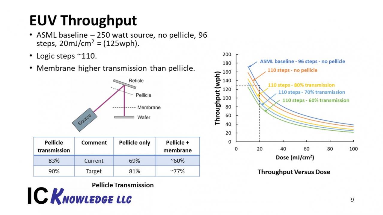
The throughput of an EUV exposure system is given by:
Exposure time = wafer overhead time + steps per wafer x (exposure time per field + stepping time)
ASML announced a few months ago that they had achieved 125 wafers per hour (wph) at a 20mJ/cm2 dose with a 250-watt source, 96 steps per wafer and no pellicle. At SPIE they announced 140wph at a 20mJ/cm2 dose with a 246-watt source, 96 steps per wafer and no pellicle. Presumably the improvement is from improved wafer overhead time and or stepping time. ASML continues to work on improving system throughput by speeding up the system and increasing source power.
These are impressive accomplishments, but:
- Logic steps are around 110
- It may be possible to expose contacts and vias without a pellicle but a pellicle will be required for metal layers and pellicles currently only transmit 83% of the EUV light.
- Photoresist doses are likely to be higher than 20mJ/cm2 at least initially.
At SPIE I presented a simple throughput model calculation based on the 125wph ASML results, see figure 1.
Figure 1. EUV throughput.
Lithographers I have talked to are predicting 30mJ/cm2 as a usable dose for 7nm logic. Greg McIntyre (director of lithography at imec) mentioned to me that he thought initial doses will be 40 or 50mJ/cm2 at 7nm or even higher.
There is a rule of thumb that cutting feature sizes in half requires 8x the dose.
As I discussed at ISS (my presentation is written up here) I expect 7nm logic to begin using EUV early next year (2019). 5nm and 6nm logic from Samsung and 5nm logic from TSMC are both due to enter preproduction in 2019 as well.
I think EUV is close to being ready for 7nm logic and that as we get high-volume manufacturing experience next year we will work though a lot of issues and likely bring doses for 7nm down to around 30mJ/cm2. The key problem in my view is that at 5nm we need doses of around 50mJ/cm2 or lower to achieve acceptable throughput on EUV tools. If the doses are 70mJ/cm2 or higher we won’t have enough EUV capacity to support the needed ramp. There is very little time to solve this problem!