Clock Domain Crossing (CDC) is a common occurrence in a multiple clock design. In the FPGA space, the number of interacting asynchronous clock domains has increased dramatically. It is normal to have not hundreds, but over a thousand clock domains interactions. Let’s assess why CDC is a lingering issue, what its impact and the available remedy guidelines to ensure a robust FPGA design.
CDC occurs whenever data is transferred from a flip-flop driven by one clock to a flip-flop driven by another clock. CDC issues could cause significant amount of failures in both ASIC and FPGA devices. The consequence of CDC is a metastability effect which leads to either functional non-determinism (unpredictability of downstream data, which could also yield to data loss) or data incoherency (when CDC induced delayed latency on subset of bus signals being sent across, causing non-uniform capture event).
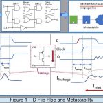
Metastability and Synchronizer — As illustrated in Figure 1, metastability may be present in design utilizing flip-flop. Any flip-flop could be made into such state by concurrent toggling of input data and sampling clock (in the diagram the concurrent switching window of the underlying gates introduced leakage current). The known approach to neutralize the effect of metastability is by the use of synchronizer. A synchronizer can be defined as a logical entity that samples an asynchronous signal and outputs a derivative signal synchronized to a local sampling clock. It is usually not synthesized, instead pre-instantiated in the design or presented as a macro. A good synchronizer should be reliable, have low latency, power and area impact. The simplest implementation is using two back-to-back flip-flops. The first flip-flop samples the asynchronous input signal into the new clock domain and waits for a full clock cycle to permit any metastability to settle down. The output signal of the first stage is sampled by the same clock into a second stage flip-flop to produce a stable and synchronized output.
Data Synchronizers — Two basic methods are available for transferring data signals across clock domain boundaries. The first is based on enable-controlled data capture in the receiving domain, while the second is based on sequential writing and reading of data using a dual-port FIFO.
Control-Based Data Synchronizers – in this type of synchronizers, the enable signal is responsible to inform the receiving domain that data is stable and ready to be captured. The transmitter is responsible for keeping data stable over time while data enable is asserted. The stability of all data bits during received data capture guarantees an absence of the metastability effect and correct data capture. Figure 2 shows variation of control based data synchronizers:
– Mux-based data synchronizer
– Enable-based data synchronizer
– Handshake-based data synchronizer
To achieve safe data capture, the control-based data synchronizer should make sender data stable, not only during period of enable signal assertion, but also covering data setup/hold margin for stability. This is key to prevent glitches during data capture. This is employed in handshake based data synchronizer.
FIFO based data synchronizer – Control based data synchronizer has limited bandwidth, while FIFO-based can increase bandwidth across the interface and still maintain reliable communication. It also allows fast data communication through clock domain boundaries. Data is pushed into the FIFO with transmitter clock and pulled out from FIFO with receiver clock. FIFO_FULL control signal manages the driver write frequency, while the FIFO_EMPTY controls the receiver read frequency.
Reset synchronizer — reset signals must be synchronized at de-assertion stage to prevent registers from going metastable with corrupted values. Reset signal edges can both be synchronized (full-synchronization) or only one (partial synchronization). Sequential elements with asynchronous reset may receive either full or partial synchronized reset, but full reset synchronizer should be targeted for sequential elements with synchronous reset.
Synchronizer in FPGA design
In FPGA design, several safety guidelines should be observed when implementing synchronizers (for more complete discussions, please refer to Aldec 17-page white paper here):
– Avoid the use of half-cycle synchronizer, which usually relies on the use of an inverted clock-edge for second-stage flop as it adds extra resources and complexity to clock implementation.
– The flip-flops (referred as NDFF, signifying 2 or more flops) should be from flip-flop FPGA resources only and should be preserved and dont-touched during synthesis, including no boundary retiming. It is preferred to use metastability hardened macros for CDC. No shift registers or BRAMs allowed as they may induce glitches. Placement of NDFF should be in the same slice to minimize inter-flop propagation delay, reducing potential metastability effects.
– In timing critical high-speed FPGA designs, avoiding combo logic at either control or data CDC is key. Due to this reason mux-based data synchronizers should be avoided. Combo logic should not be injected between synchronizer stages or CDC.
– Ensure no clock reconvergence in the receiving domain even after one or more register stages. Also use synchronizers that match with your data transfer speed needs. For IP developers, it is better to contain the CDC transition within the IP design, avoiding uncontrolled data latency from outside the block.
– FPGA vendors (Xilinx, Intel) based flows utilized attribute reserved for indicating the NDFF flip-flops structure. This attribute will prompt the underlying tools in the flow to react accordingly. It will trigger the synthesis tool to apply “dont_touch” on the synchronized flops and instruct the placement tool to place these flops in close proximity preferably in one slice, although not necessarily all synchronizers implemented in slices. Apply key SDC constraints such as set_max_delay instead of set_false_path to CDC related timing paths to the interface. There are variations also in how the downstream tools respond to the attribute, such as different handling of X state generation depending which vendor solution is used. It is also necessary for timing analysis to not consider the path from upstream driver flop to this NDFF structure, by setting proper constraint.
For non-timing-critical FPGA designs, use BRAM’s instead of driving a flip-flop array, to connect directly to receiving flip-flops from another clock domain. To avoid glitch during data transfer, output of BRAM should remain stable during enable signal assertion (also sufficient margin for setup and hold).
Built-in FIFO generators such as LogicCORE IP FIFO Generator from Xilinx can be used to implement safe FIFO-based data synchronizers for FPGA. The generated FIFO should be configured with independent clocks for read and write operations. For custom-built FIFOs, it is important to check that read and write pointers crossing clock-domains are properly encoded, with only one bit changing a time (just like Greycode) and validated by assertion.
CDC Sign-off — Achieving CDC sign-off in today’s FPGA designs is as crucial as functional correctness and timing closure. The existing dominating CDC verification methods/tools designated for the ASIC flow need to be retargeted to be efficient in the context of FPGA. The ALDEC_CDC rule plug-in turns ALINT-PRO into a full-scale CDC and RDC Verification solution capable of complex clock and reset domain crossings analysis and handling of metastability issues in multi-clock and multi-reset designs. The verification strategy in ALINT-PRO is comprised of static structural verification, design constraints setup, and dynamic functional verification. The first two steps are executed in ALINT-PRO, while dynamic checks are implemented via integration with simulators (Riviera-PRO™ , Active-HDL™, and ModelSim® are supported) based on the automatically generated testbench. This approach reveals potential metastability problems during RTL simulation, which otherwise would require lab tests to be detected. Debugging CDC and RDC issues is being achieved via rich schematic and cross-probing mechanisms, as well as comprehensive reports and TCL-based API, which allows browsing through synthesis results, clocks and resets structures, detected clock and reset domain crossings, and identified synchronizers.
For more info on ALDEC Static Design Verification ALINT-PRO, please refer to this link or download the white paper Clock Domain Crossings in the FPGA World.