To borrow a punch line from Duke professor Dan Ariely, artificial intelligence is like teenage sex: “Everyone talks about it, nobody really knows how to do it, everyone thinks everyone else is doing it, so everyone claims they are doing it.” Even though AI systems can now learn a game and beat champions within hours, they are hard to apply to business applications.
M.I.T. Sloan Management Review and Boston Consulting Group surveyed 3,000 business executives and found that while 85 percent of them believed AI would provide their companies with a competitive advantage, only one in 20 had “extensively” incorporated it into their offerings or processes. The challenge is that implementing AI isn’t as easy as installing software. It requires expertise, vision, and information that isn’t easily accessible.
When you look at well known applications of AI like Google’s AlphaGo Zero, you get the impression it’s like magic: AI learned the world’s most difficult board game in just three days and beat champions. Meanwhile, Nvidia’s AI can generate photorealistic images of people who look like celebrities just by looking at pictures of real ones.
AlphaGo and Nvidia used a technology called generative adversarial networks, which pits two AI systems against each another to allow them to learn from each other. The trick was that before the networks battled each other, they received a lot of coaching. And, more importantly, their problems and outcomes were well defined.
Most business problems can’t be turned into a game, however; you have more than two players and no clear rules. The outcomes of business decisions are rarely a clear win or loss, and there are far too many variables. So it’s a lot more difficult for businesses to implement AI than it seems.
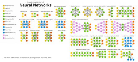
Today’s AI systems do their best to emulate the functioning of the human brain’s neural networks, but they do this in a very limited way. They use a technique called deep learning, which adjusts the relationships of computer instructions designed to behave like neurons. To put it simply, you tell an AI exactly what you want it to learn and provide it with clearly labelled examples, and it analyzes the patterns in those data and stores them for future application. The accuracy of its patterns depends on data, so the more examples you give it, the more useful it becomes.
Herein lies a problem: An AI is only as good as the data it receives. And it is able to interpret that data only within the narrow confines of the supplied context. It doesn’t “understand” what it has analyzed, so it is unable to apply its analysis to scenarios in other contexts. And it can’t distinguish causation from correlation. AI is more like an Excel spreadsheet on steroids than a thinker.
The bigger difficulty in working with this form of AI is that what it has learned remains a mystery — a set of indefinable responses to data. Once a neural network is trained, not even its designer knows exactly how it is doing what it does. As New York University professor Gary Marcus explains, deep learning systems have millions or even billions of parameters, identifiable to their developers only in terms of their geography within a complex neural network. They are a “black box,” researchers say.
Speaking about the new developments in AlphaGo, Google / DeepMind CEO Demis Hassabis reportedly said, “It doesn’t play like a human, and it doesn’t play like a program. It plays in a third, almost alien, way.”
Businesses can’t afford to have their systems making alien decisions. They face regulatory requirements and reputational concerns and must be able to understand, explain, and demonstrate the logic behind every decision they make.
For AI to be more valuable, it needs to be able to look at the big picture and include many more sources of information than the computer systems it is replacing. Amazon is one of the few companies that has already understood and implemented AI effectively to optimize practically every part of its operations from inventory management and warehouse operation to running data centers.
In inventory management, for example, purchasing decisions are traditionally made by experienced individuals, called buyers, department by department. Their systems show them inventory levels by store, and they use their experience and instincts to place orders. Amazon’s AI consolidates data from all departments to see the larger trends — and relate them to socioeconomic data, customer-service inquiries, satellite images of competitors’ parking lots, predictions from The Weather Company, and other factors. Other retailers are doing some of these things, but none as effectively as Amazon.
This type of approach is also the basis of Echo and Alexa, Amazon’s voice-based home appliances. According to Wired, by bringing all of its development teams together and making machine learning a corporate focus, Amazon is solving a problem many companies have: disconnected islands of data. Corporate data are usually stored in disjointed datasets in different computer systems. Even when a company has all the data needed for machine learning, they usually aren’t labelled, up-to-date, or organized in a usable manner. The challenge is to create a grand vision for how to put these datasets together and use them in new ways, as Amazon has done.
AI is advancing rapidly and will surely make it easier to clean up and integrate data. But business leaders will still need to understand what it really does and create a vision for its use. That is when they will see the big benefits.
For more, you can read my book Driver in the Driverless Car