At the Silicon Valley SNUG 2018, Synopsys Chairman and co-CEO Dr. Aart de Geuss gave his keynote speech addressing attendees on how far we have evolved, and at times encountered the aha factor that helps propel us to the next level. He explored trends as well as the current state of his company solution offerings.
Moore’s Law, Digital Twin and Security
Aart gave snapshots on how the Synopsys synthesis product (Design Compiler) was incepted in 1986 and called SOCRATES which stands for Synthesis and Optimization of Combinatorial logic using Rule-based And Technology independent Expert System. He quipped that it already contains some intelligent aspects and pointed out that it has three main interacting components timing, library and synthesis.
Next, he noted that the progression steps towards automation usually involves capturing the concept or requirements, followed by modeling it, then simulate, analyze the results and subsequently find ways to optimize and eventually automate it. He indicated that the March of Moore’s Law although slower and more expensive is still occurring towards the 5nm process node. Aart said that the device structure is more “funky”, one could see the interfaces with only few atomic layers. He alluded to the importance of having a digital-twin, a replica of the design or system one’s building. He gave few examples along this line. First on how GE was able to build and simulate the operation of a turbine, jet engine and applied various conditions for a period of time simulating its usage in the field, and being able to identify potential failure spots. Designer could use Synopsys virtual prototyping and performed some analysis on his design prior to the end of its implementation. With the current tool offering, one could also build new device, build the cell, simulate and characterize its timing.
Security is also crucial and getting more attention as systemic complexity and ownership demand measures to respond upon vulnerability to attacks. To this end, Synopsys offers solutions from its acquired security companies: Coverity to address code static analysis; Black Duck to address software composition analysis; and Seeker to address dynamic analysis (a debugging method that evaluates a program during execution). The last one can be used to verify vulnerability during runtime. To illustrate his case, Aart showed four access scenarios that correspond to the four quadrants.
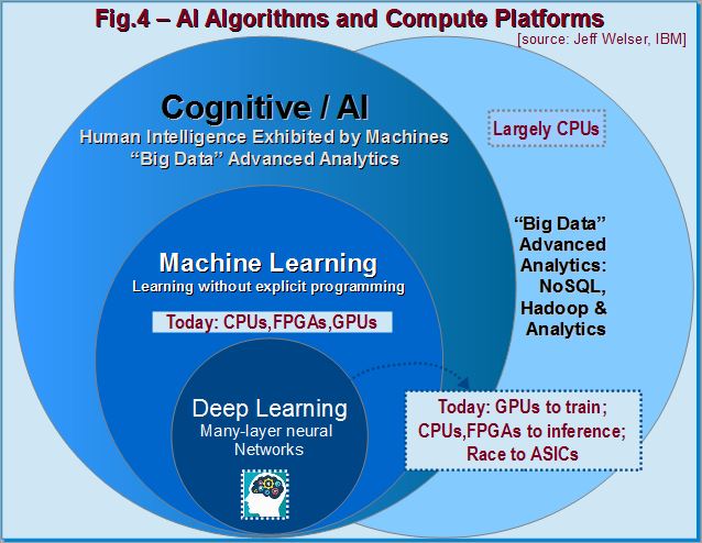
The rise of AI
Aart provided a flashback using slides on how we got here. During the millenium phase: with agriculture and tooling time; followed by the century phase with the steam engine and industrial revolution; then by our recent decades in which we have physical (computing), biological (mobility), and finally at the present time by intellectual (smart everything). The increased valuation resulted from the last inflection points which occurred during the past decades:
● 100B – AI: IoT, Big Data, ML
● 50B – Compute: PC, Internet, Networking Server, Cloud
● 25B – Mobility: phone, smartphones, social media
Just like the invention of the printing press and the use of the alphabet, we are harnessing AI and the digitization of things through a binary-logic concept to create design. “Systemic understanding blossoming worldwide”, he said. Applications such as autonomous vehicles, although not perfected (with recent fatality incidents) and raises ownership as well as privacy issues on the massive amount of data being generated. This has accelerated the impact on compute power, demanding faster performance. He touted that you have to be fast in order to solve the fast-performance demand. He highlighted the company photonic design solution which was complemented recently through the acquisition of Phoenix B.V. The acquisition enables Synopsys to enhance the current photonics design automation in handling physical layout capabilities.
He added that on the path from capture to automation, AI (through machine learning) will add learning and interpretation at the interface of the analysis and the optimization steps. Iterating on the interface is where the action is. He highlighted Synopsys current tool offering as being a total fusion. Previously the company introduced Common Platform which as a framework for synthesis, P&R, STA and extraction. Now Fusion offers four types: Design, ECO, Signoff and Test. In Design Fusion, a tight usage correlation is achieved between Design Compiler and the ICC2 tool. The integration provides a few percentage gains in both power and area, on a hard-to-close timing design. Another fusion example is ECO Fusion which enables PrimeTime and Star-RC/XT usage in ICC2. Ongoing and future works will involve folding in machine learning for additional QoR and improved TTR (Time to Results).
Aart also shared the status of the first Synopsys collaboration with ANSYS in bundling the RedHawk analysis tool in a fusion-like approach to address power integrity analysis within the ICC2 implementation stage. He shared a roadmap towards providing a complement set of features from ANSYS toward midyear.
Aart stated that we have the privilege to be in the middle of profound changes –changes that will impact on our lives and the lives of our children presenting big opportunities, absolutely. In closing he thanked everyone for their continued support.