Nvidia has an affinity for taking on computational challenges. Whether it be diagnostic tools derived from medical imaging, mapping the earth’s core or defining the structure of HIV, Nvidia is there with GPU computational resources to amp up the teraflops and shrink the computing time. In fact, according to Nvidia’s most recent earnings report, GPUs are increasingly being turned to by the leading creators of supercomputers in the U.S. and Japan.
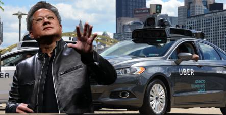
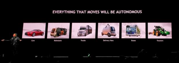
The automotive industry has brought Nvidia the toughest test yet, in the words of Nvidia CEO Jensen Huang, in the form of mastering automated driving. In the midst of regulatory and legislative battles over self-driving technology, Nvidia has stepped forward with a clear path toward solving the problem and closing the gap between current and future safe autonomous vehicle performance.
Regulators and politicians may pontificate about autonomous technology but Nvidia is getting down to business. Nvidia is in a unique position to solve the problem as a public company at the center of an ecosystem of 370 development partners (and growing) all working on the autonomous driving challenge. Nvidia brings to that challenge a portfolio of hardware, software, servers, code libraries and technicians all working toward the same objective in real-time in the real world.
The implications of Nvidia’s market position are most significant because the challenge shared by all is getting, in the words of Nvidia CEO Jensen Huang, “from 1 million miles to 1 trillion miles.” To achieve any level of confidence in an automated driving system, developers will need to drive or simulate driving hundreds of billions of miles. If there is a company on the planet that knows anything about simulation, it is Nvidia.
In his keynote at GTC 2018 in San Jose this week, the Nvidia CEO picked up the automated driving gauntlet signifying Nvidia’s intention to conquer that challenge with new tools in the form of its DRIVE Constellation – a computing platform based on two different servers.
The first server runs Nvidia DRIVE Sim software to simulate a self-driving vehicle’s sensors, such as cameras, lidar and radar. The second contains a powerful Nvidia DRIVE Pegasus AI car computer that runs the complete autonomous vehicle software stack and processes the simulated data as if it were coming from the sensors of a car driving on the road.
Autonomous vehicle creators like Waymo and Cruise have been able to rack up single digit millions of miles from the dozens or hundreds of test vehicles they have been able to put on roads. But the weakness of this brute force method is manifest in the individual on-road mishaps and, in the case of Uber just last week, fatalities that result from unanticipated scenarios or system failures.
Automotive industry safety standards allow little or no room for failure and here, too, Nvidia is a leader. Huang says the Nvidia line up represents “the first line up of computers that Nvidia has ever made that stands up to the highest standard of functional safety ISO 26262 and ASIL-D. It is the first time that we have delivered this level of software and hardware complexity.” In fact, Huang describes the earlier announced Xavier as “the most complex SoC the world has ever created.”
One might wonder what Nvidia’s reward has been for the millions of dollars the company is pouring into the development of these self-driving compute platforms. The reality is that Nvidia’s shift in focus from automotive infotainment systems to autonomous driving technology has been almost as challenging as the process of creating those new systems.
Gaming, datacenters and professional visualization remain the dominant portions of Nvidia’s business. Revenue growth for automotive in the most recent quarter was a disappointing 3% and down sequentially as a result of this transition from infotainment to safety. Driving automation appears to be the correct bet for Nvidia, but it’s clearly a long-term play.
Nvidia’s commitment, though, is clear and deep – maybe that’s because the company sees a trillion-dollar opportunity, according to Huang. Presenters at the GTC event in San Jose are sharing papers on everything from object detection to driver monitoring with the common threads being the application of artificial intelligence and deep learning with Nvidia’s help. It would be hard to find a more technically oriented event focusing on automated driving anywhere in the world.
The scope of Nvidia’s comprehension of the task and CEO Huang’s grasp of the nitty gritty details was manifest in the closing segment of his keynote yesterday which focused on a virtualization exercise enabling a remote driver to guide a driverless vehicle. Huang called the audience’s attention to a fact that few have grasped that autonomous vehicles will require remote operation and control – a solution to which Nvidia has already created.
The only issue unaddressed by Nvidia’s impressive presentation was the special role the company is playing in the automation of driving. At a time when car companies and their suppliers are just beginning to come to grips with the need to share information and even vehicle data, Nvidia is in a unique position to create a data sharing platform to further accelerate the advancement of autonomous vehicle technology.
Nvidia’s Huang gave only the slightest hint of such a prospect. With 370 partners – and growing – it will be hard for the company to ignore the opportunity. It may even be something that partners seek out or that regulators require. Shrinking the 1M-to-1T gap will require more than simulation – it will require collaboration and data sharing. Huang made a single comment regarding the prospect of “opening up” Nvidia’s data sets during an analyst Q&A at the end of the day yesterday. Time will tell whether this is part of Nvidia’s solution to what may be its greatest challenge ever.