If you are like me, you will get a 5G phone because of the high bandwidth it offers. However, there is a lot more to 5G than just fast data. In fact, one of the appealing features of 5G is low bandwidth communication. This is useful for edge devices that perform infrequent and low volume data transfers and depend on long battery life. Prior to 5G many devices relied on 2G or 3G for data transfer which came with very high power requirements and costs, due to cellular overhead. 5G adds support for Narrow Band IoT (NB-IoT) communication for power sensitive devices.
However, simply taking a radio architecture designed for higher bandwidth and applying it to NB-IoT leaves a lot to be desired. The best analogy I can come up with is why SUVs initially drove like trucks. If you take a truck chassis and build an SUV on it, what you will get is a car that rides like a truck.
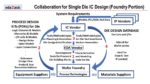
Synopsys does a good job of highlighting this in a recent webinar video that introduces their new NB-IoT ARC Communications IP Subsystem for Wireless Narrowband IoT designs. The video was done in conjunction with Santa Clara based Palma Ceia Semidesign who collaborated with Synopsys to develop a complete hardware/software NB-IoT Solution. Rich Collins, PMM at Synopsys for ARC Processors & Subsystems starts by describing what is new and different about 5G’s NB-IoT.
Rather than take a wide band cellular LTE modem and adapt it to NB-IoT, Synopsys has taken the approach of eliminating unnecessary hardware and moving much of the functionality into software running on a specifically designed processor. This has many advantages. There is a shortened development cycle for the smaller hardware implementation. It is also more flexible and can easily be adapted to changing standards. Synopsys provides a full software kit to support Base Comms and the NB-IoT User Equipment Stack.
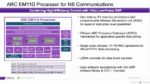
The processor at the heart of this Subsystem is the ARC EM11D. It combines high efficiency control with ultra low power DSP operations. Its ARC Processor EXtension (APEX) mechanism is useful for adding application specific extensions in the form of hardware RTL. It features a single cycle 16+16 MAC that efficiently supports PHY data processing. There is also a development library with rich DSP functions.
The NB-IoT subsystem has many features that enable low power communications. The Digital Front End facilitates integration with RF transceivers. Viterbi and trig functions are handled in hardware through APEX instructions. There are standard AHB/APB busses that help with SoC integration. There are also standard peripheral interfaces that can be used for power management, as well as RF and host connectivity. The subsystem also possesses flexible power management features with customer programmable power modes.
Rich talks about the needs of a complete IoT SoC using their IP based system concept. The IoT comms subsystem is combined with tRoot HSM for iSIM to provide SIM functionality and security. An RF transceiver, such as the Palma Ceia PCS NB-IoT Transceiver, eFlash and RAM/ROM round out the system, providing everything needed for a fully functional IoT SoC that can use 5G networks and have standby battery life of over 10 years.
At the end of the webinar Rich discusses a demo platform they assembled that shows the feasibility of the complete solution. 5G NB-IoT will be used in medical/fitness devices, smart cities, smart agriculture, industrial automation and many other applications. With the roll out of 5G, NB coverage will be available in places that never had low cost and low power service. There is rapid adoption in the US, Europe and Asia. Undoubtably there will be a high demand for SoCs that support NB-IoT. I’d suggest the Synopsys/Palma Ceia webinar video to anyone who has an interest in this topic. It is available on the Synopsys website and goes into much more detail on the ARC Communications IP Subsystem and RF transceiver.