webinar banner AI 2026 v2

Inside the HP Nanoprocessor: A High-speed Processor That Can’t Even Add

Inside the HP Nanoprocessor: A High-speed Processor That Can’t Even Add
by Ken Shirriff on 09-06-2020 at 10:00 am

Inside the HP Nanoprocessor

The Nanoprocessor is a mostly-forgotten processor developed by Hewlett-Packard in 19741 as a microcontroller2 for their products. Strangely, this processor couldn’t even add or subtract,3 probably why it was called a nanoprocessor and not a microprocessor. Despite this limitation, the Nanoprocessor powered numerous Hewlett-Packard devices ranging from interface boards and voltmeters to spectrum analyzers and data capture terminals.4 The Nanoprocessor’s key feature was its low cost and high speed: Compared against the contemporary Motorola 6800,7 the Nanoprocessor cost $15 instead of $360 and was an order of magnitude faster for control tasks.

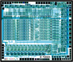
Recently, the six masks used to manufacture the Nanoprocessor were released by Larry Bower, the chip’s designer, revealing details about its design. The composite mask image below shows the internal circuitry of the integrated circuit.5 The blue layer shows the metal on top of the chip, while the green shows the silicon underneath. The black squares around the outside are the 40 pads for connection to the IC’s external pins. I used these masks to reverse-engineer the circuitry of the processor and understand its simple but clever RISC-like design.6

Combined masks from the Nanoprocessor. Click for larger image. “GLB“, to the left of the data bus, stands for the designers George Latham and Larry Bower. Files courtesy of Antoine Bercovici.

The Nanoprocessor was designed in 1974, the same year that the classic Intel 8080 and Motorola 6800 microprocessors were announced. However, the Nanoprocessor’s silicon fabrication technology was a few years behind, using metal-gate transistors rather than silicon-gate transistors that were developed in the late 1960s. This may seem like an obscure difference, but silicon gate technology was much better in several ways. First, silicon-gate transistors were smaller, faster, and more reliable. Second, silicon-gate chips had a layer of polysilicon wiring in addition to the metal wiring; this made chip layouts about twice as dense.8 Third, metal-gate circuitry required an additional +12 V power supply. The Intel 4004 processor used silicon gates in 1971, so I’m surprised that HP was still using metal gates in 1974.9

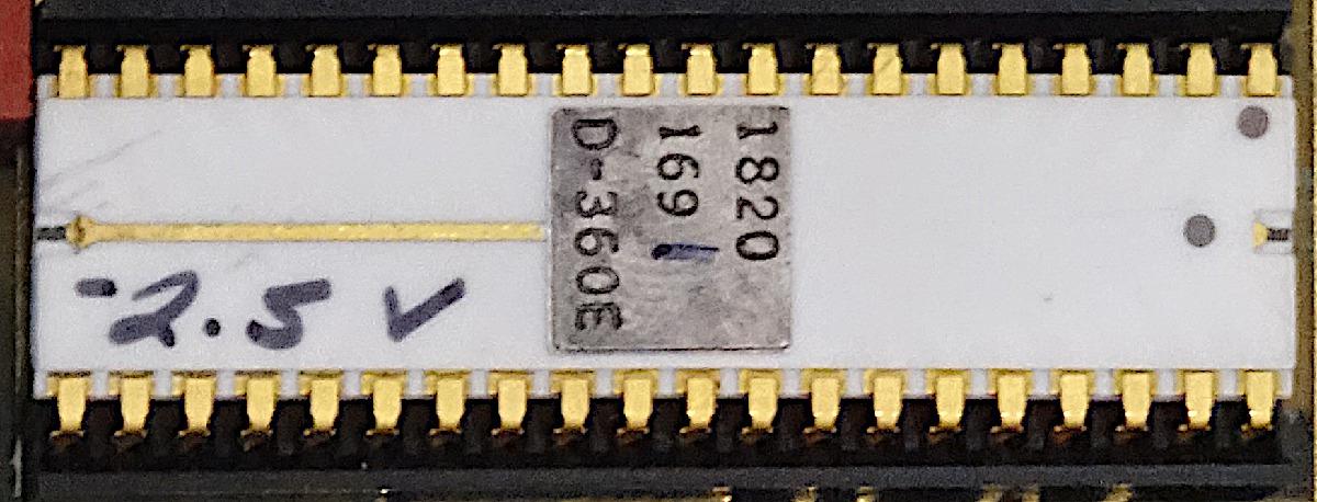
A bizarre characteristic of the Nanoprocessor is its variable substrate bias voltage. For performance reasons, many 1970s microprocessors applied a negative voltage to the silicon substrate, with -5V provided through a bias pin.10 The Nanoprocessor has a bias pin, but strangely the bias voltage varied from chip to chip, from -2 volts to -5 volts. During manufacturing, the required voltage was hand-written on the chip (below). Each Nanoprocessor had to be installed with a matching resistor to provide the right voltage. If a Nanoprocessor was replaced on a board, the resistor had to be replaced as well. The variable bias voltage seems like a flaw in the manufacturing process; I can’t imagine Intel making a processor like that.

The HP Nanoprocessor, part number 1820-1691. Note the hand-written voltage “-2.5 V”. The last digit (1) of the part number is also hand-written, indicating the speed of the chip. Photo courtesy of Marc Verdiell.

Like most processors of that era, the Nanoprocessor was an 8-bit processor. However, it didn’t use RAM, but ran code from an external 2-kilobyte ROM. It contained 16 8-bit registers, more than most processors and enough to make up for the lack of RAM in many applications. Based on transistor count, the Nanoprocessor is more complex than the Intel 8008 (1972) and slightly less complex than the 6800 (1974) or 6502 (1975).11 Its architecture uses its transistor count on different purposes from these processors, though. The Nanoprocessor lacks ALU functionality but in exchange, it has a large register set, taking up much of the die area. The Nanoprocessor has 48 instructions, a considerably smaller instruction set than the 6800’s 72 instructions. However, the Nanoprocessor includes convenient bit set, clear, and test operations, which these other processors lacked.12 The Nanoprocessor supports indexed register access, but lacks the complex addressing modes of the other processors.

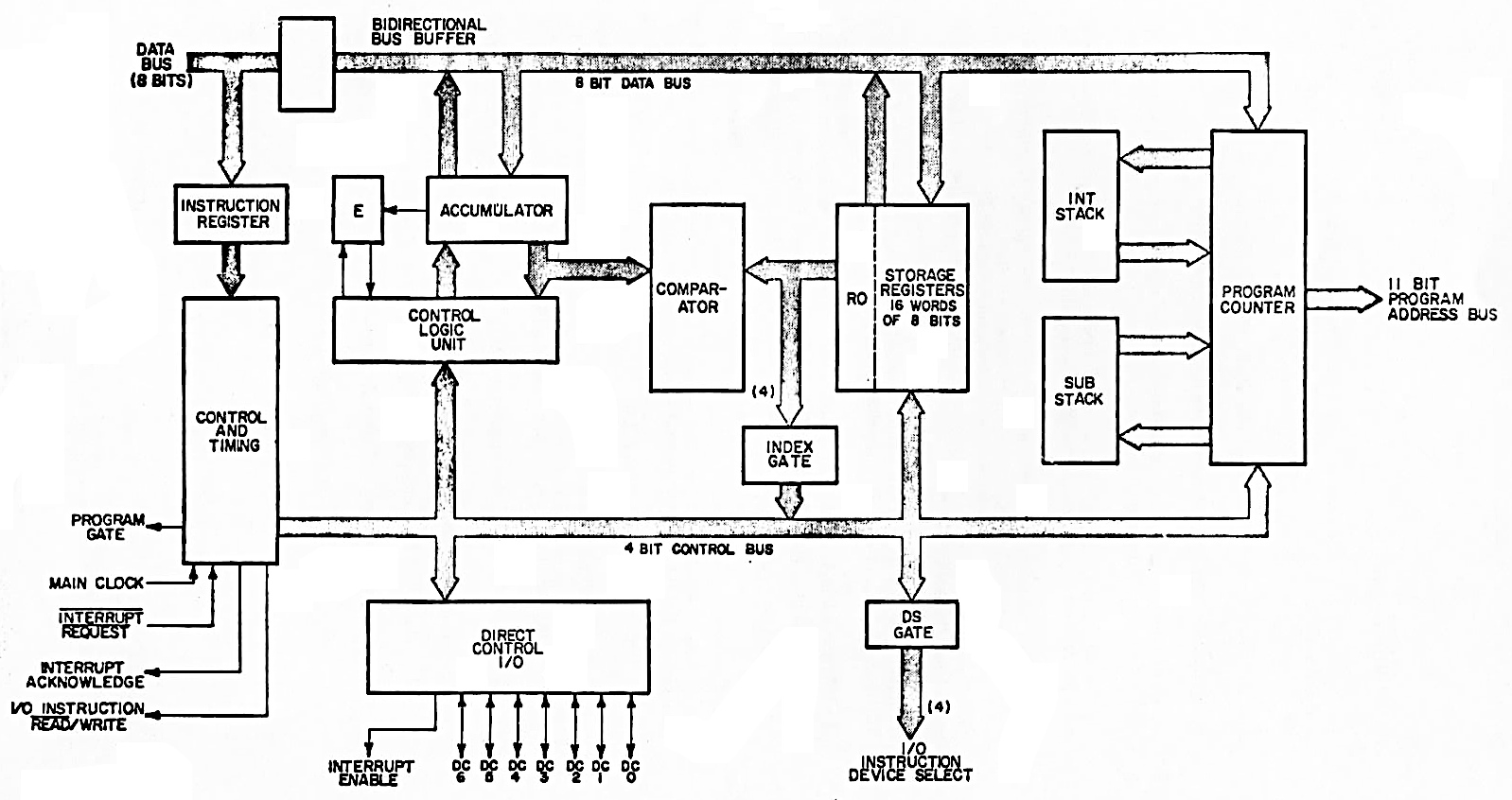
The block diagram below shows the internal structure of the Nanoprocessor. The main I/O feature is the 4-bit “I/O Instruction Device Select” which allows 15 devices to receive I/O operations. In other words, the select pins indicate which I/O device is being read or written over the data lines. External circuitry uses these signals to do whatever is necessary for the particular application, such as storing the data in a latch, sending it to another system, or reading values. More I/O is provided through seven “Direct Control I/O” pins (GPIO pins) that can be used for inputs or outputs. If not connected to external circuitry, these pins operate as convenient bit flags; the Nanocomputer can set a value and then read it back. The Control Logic Unit performs increments, decrements, shifts, and bit operations on the accumulator, lacking the arithmetic and logical operations of a standard Arithmetic/Logic Unit (ALU).

Block diagram, from the Nanoprocessor User’s Guide.


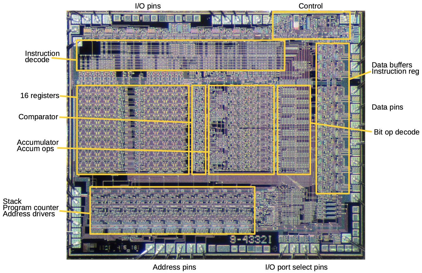
I reverse-engineered the Nanoprocessor’s circuitry from the masks and determined how the functional blocks map onto the die, below. The largest feature is the set of 16 registers in the center-left. To the right is the comparator and then the accumulator, along with its increment, decrement, shift, and complement circuitry. The instruction decoder circuitry takes up much of the space above and to the right of the comparator and accumulator. The bottom part of the chip is dominated by the 11-bit program counter, along with the one-entry interrupt stack and subroutine stack. The control circuitry implements the Nanoprocessor’s almost-trivial instruction timing: one fetch cycle followed by one execute cycle.13 In most microprocessors, the control circuitry takes up a large fraction of the chip, but the Nanoprocessor’s control circuitry is just a small block.

Functional components of the HP Nanoprocessor, based on my reverse-engineering. Underlying die photo by Pauli RautakorpiCC BY 3.0.


Understanding the masks

The chip was fabricated using six masks, each used for constructing one layer of the processor using photolithography. The photo below shows the masks; each one is a 47.2×39.8 cm Mylar sheet. These sheets are 100× enlargements of the masks used to produce the 4.72×3.98 mm silicon die (for comparison, about 33% smaller than the 6800’s die). Each 3-inch silicon wafer held about 200 integrated circuits, fabricated together on the wafer, and then tested, cut apart, and packaged.

The chip’s masks, courtesy of Antoine Bercovici


To explain the role of the masks, I’ll start with the structure of a metal-gate MOSFET, the transistor used in the Nanoprocessor. At the bottom, two regions of silicon (green) are doped to make them conductive, forming the source and drain of the transistor. A metal strip in between forms the gate, separated from the silicon by a thin layer of insulating oxide. (These layers—Metal, Oxide, Semiconductor—give the MOS transistor its name.) The transistor can be considered a switch controlled by the gate. The metal layer also provides the main wiring of the integrated circuit, although the silicon layer is also used for some wiring.

Structure of a metal-gate MOSFET.


Masks are a key part of the integrated circuit construction process, specifying the position of the components. The diagram below shows how a mask is used to dope regions of the silicon. First, the silicon wafer is oxidized to form an insulating oxide layer on top, and then light-sensitive photoresist is applied. Ultraviolet light polymerizes and hardens the photoresist, except where the mask blocks the light. Next, the soft, unexposed photoresist is dissolved. The wafer is exposed to hydrofluoric acid, which removes the oxide layer where it is not protected by photoresist. This yields holes in the oxide that match the mask pattern. The wafer is then exposed to a high-temperature gas which diffuses into the unprotected silicon regions, modifying the silicon’s conductivity. These processing steps create tiny doped silicon regions matching the masks’s pattern. As will be shown below, the other masks are used for different processing steps, but using the same photoresist-and-mask process.

How a photomask is used to dope regions of silicon.


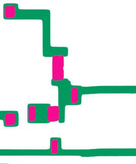
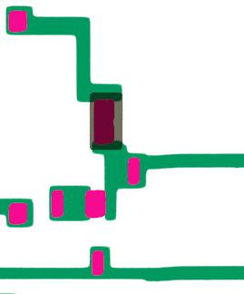
I’ll zoom in on the Nanoprocessor’s die and show how one of its circuits is constructed from the six masks. (This two-transistor circuit is an inverter, flipping the binary value of its input.) The first mask dopes regions of silicon to make them conductive, using the photolithography steps described above. The doped regions (green) will become transistor source/drains or wiring between components.

The first mask creates conductive silicon regions.

Next, the die is covered with an insulating oxide layer. The second mask (magenta) is used to etch openings in the oxide, exposing the silicon underneath. These openings will be used to create transistor gates as well as connecting metal wiring to the silicon.

The second mask creates openings in the oxide layer.

The third mask (gray) exposes a region to ion implantation, which changes the doping of the silicon, and thus the transistor’s properties. This turns the upper transistor into a special depletion-mode transistor that pulls logic gate outputs high.

The third mask is used to increase the doping of the upper transistor.


Next, the silicon is covered with an additional thin layer of insulating oxide, forming the gate oxide for the transistors. The fourth mask (orange) removes this oxide from regions that will become contacts between the silicon and the metal layer. After this step, most of the die is covered with a thick insulating oxide layer. The oxide layer is very thin over the transistor gates (magenta), and there are contact holes in the oxide from the current mask (orange).

The fourth mask creates holes in the oxide.


The fifth mask (blue) is used to create the metal wiring on top; a uniform metal layer is applied and then the undesired parts are etched off. In locations where the fourth mask created holes in the oxide, the metal layer contacts the silicon and forms a connection. In locations where the third mask created a thin oxide layer, the metal layer forms the transistor gate between two silicon regions. Finally, the entire wafer is covered with a protective glassy layer. The sixth mask (not shown) is used to form holes in this layer over the pads around the edges of each chip. Once the wafer is cut into individual silicon dies (dice?), bond wires are attached to the pads, connecting the die to the external pins.

The fifth mask creates the metal wiring.


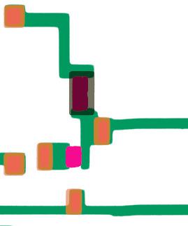
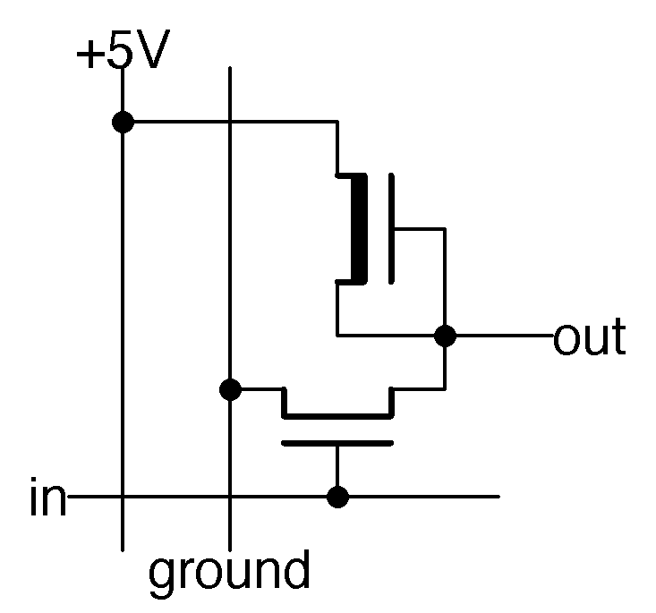
The schematic below shows how the circuitry above forms a two-transistor inverter. The two transistor symbols correspond to the two transistors created by the masks. When there is no input, the upper transistor (connected to +5 volts) pulls the output high. When the input is high, it turns on the lower transistor. This connects the output to ground, pulling the output low. Thus, the circuit inverts the output.

Schematic of an NMOS inverter, corresponding to the masks above.


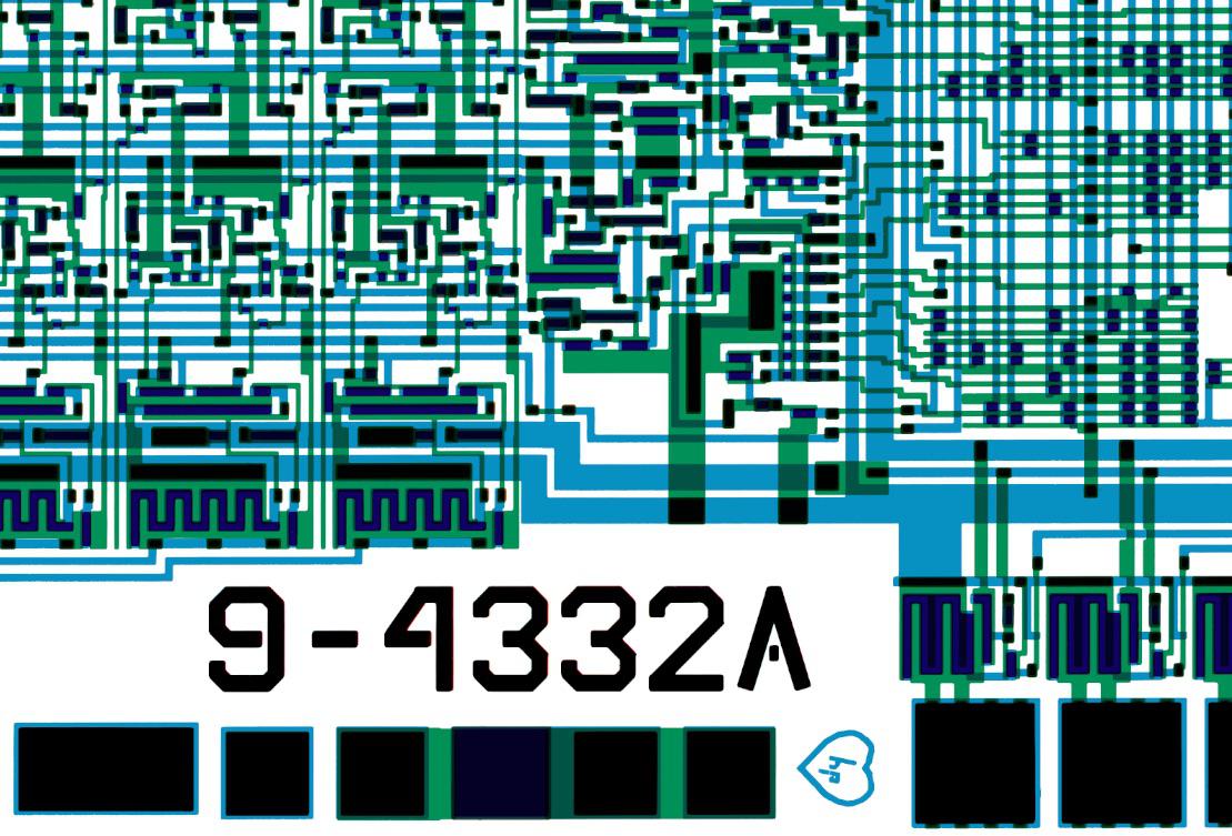
Although the diagrams above show just a single inverter, these masking steps create the entire processor with its 4639 transistors.11 The diagram below shows a larger part of the die with dozens of transistors forming more complex gates and circuitry. One cute thing I noticed on the masks is a tiny heart with HP inside, below the chip’s number.14

Chip art: HP inside a heart, below the part number 9-4332A

Controlling a clock with the Nanoprocessor

To understand how the Nanoprocessor was used in practice, I reverse-engineered the code from an HP 98035 clock module. This module was plugged into an HP desktop computer15 to provide a real-time clock, as well as millisecond-accurate timings, intervals, and periodic events. The design of the clock module was rather unusual. To preserve the time when the computer was powered-down, the clock module was built around a digital watch chip with a backup battery.17 Inconveniently, the digital watch chip wasn’t designed for computer control: it generated 7-segment signals to drive an LED, and it was set through three buttons. To read the time, the Nanoprocessor had to convert the 7-segment display outputs back into digits. And to set the time, the Nanoprocessor had to simulate the right sequence of button presses to advance through the digits.

Nanoprocessor (white chip) as part of an HP clock module. The 2-kilobyte ROM is to the left of the Nanoprocessor. The two 256-bit×4 RAM chips are to the right. The Texas Instruments clock chip is the large black chip below the green NiCad battery. Photo courtesy of Marc Verdiell.


The host computer controlled the clock module by sending it ASCII strings such as “S 12:07:12:45:00” to set the clock to 12:45:00 on December 7 (or on July 12 if the module was running in European mode). The module’s various interval timers, periodic alarms, and counters were controlled with similar commands such as “Unit 2 Period 12345”. The module supported 24 different commands, and the Nanoprocessor had to parse them. (See the manual for details.)

Here’s some sample code reverse-engineered from the clock board ROM. This code is from the interrupt handler that increases the time and date every second. The code below determines how many days in the current month so it knows when to move to the next month. The columns are the byte value, the corresponding opcode, and my description of the instruction.

d0 STR-0 Store the next byte (7) in register 0.
07
0c SLE Skip two instructions if accumulator <= register 0.
03 DED Decrement the accumulator in decimal mode
5f NOP No operation
d0 STR-0 Store the next byte (0x31) in register 0
31
30 SBZ-0 Skip two instruction bytes if accumulator bit 0 is zero
81 JMP-1 Jump to 0x1c9 (end of this code block)
c9
a1 CBN-1 Clear accumulator bit 1
d0 STR-0 Store the next byte (0x30) in register 0
30
0f SAN Skip two instruction bytes if accumulator not zero
d0 STR-0 Store next byte (0x28) in register 0
28
view rawdays-in-month hosted with ❤ by GitHub


This code takes a month number (01-12 BCD) in the accumulator and returns (in register 0) the number of days in the month (28, 30, or 31 BCD). Not bad for 16 bytes of code, even if it ignores leap years. How does it work? For months past 7 (July), it subtracts 1. Then, if the month is odd, it has 31 days, while an even month has 30 days. To handle February, the code clears bit 1 of the month. If the month is now 0 (i.e. February), it has 28 days.

This code demonstrates that even though a processor without addition sounds useless, the Nanoprocessor’s bit operations and increment/decrement allow more computation than you’d expect.16 It also shows that Nanoprocessor code is compact and efficient. Many things can be done in a single byte (such as bit test and skip) that would take multiple bytes on other processors.12 The Nanoprocessor’s large register file also avoids much of the tedious shuffling of data back and forth often required in other processors. Although some call the Nanoprocessor more of a state machine controller than a microprocessor, that understates the capabilities and role of the Nanoprocessor.

While the Nanoprocessor doesn’t include an ALU or have instructions for accessing RAM, these could be added as I/O devices. The clock module has 256 bytes of RAM to hold its multiple counter and timer values, accessed through four I/O ports. Other products added ALU chips to support arithmetic operations.18

Conclusions

The Nanoprocessor is an unusual processor. My first impression was that it wasn’t even a “real processor”, lacking basic arithmetic functionality. The chip was built with obsolete metal-gate technology, a few years behind other microprocessors. Most bizarrely, each chip required a different voltage, hand-written on the package, suggesting difficulty with manufacturing consistency. However, the Nanoprocessor provided high performance in its microcontroller role, much faster than other processors at the time. Hewlett-Packard used the Nanoprocessor in many products in the 1970s and 1980s, in roles that were more complex than you’d expect. strings and performing calculations.

While the Nanoprocessor has languished in obscurity, without even a mention on Wikipedia, the masks recently revealed by its designer shed light on this unusual corner of processor history. Thanks to Antoine Bercovici for scanning and remastering the masks, Larry Bower for the donation, and John Culver at The CPU Shack for sharing the donation. Thanks to Marc Verdiell for dumping the clock board ROM.

I plan to write about the internal circuitry of the Nanoprocessor so follow me on Twitter at @kenshirriff for updates on Part II. I also have an RSS feed.

Notes and references

  1. More information on the HP Nanoprocessor and its history is in CPU Shack’s recent article The Forgotten Ones: HP Nanoprocessor, as well as at HP9825.com and The HP 9845 Project
  2. I’m not completely comfortable calling the Nanoprocessor a microcontroller since it uses an external program ROM, while a microcontroller usually has everything, including the ROM, on a single chip. (It is like the Intel 4004 in this way.) However, the Nanoprocessor resembles a microcontroller in most ways: it is designed for embedded control applications, with a Harvard architecture and an instruction set optimized for I/O, running a program from ROM with minimal storage. 
  3. On the topic of computers that can’t add, the desk-sized IBM 1620 computer (1959) didn’t have addition circuitry, but used table lookup for addition. It had the codename CADET; people joked that this stood for “Can’t Add, Doesn’t Even Try.” 
  4. I’ve determined that the Nanoprocessor was used in the following HP products (and probably others): HP 9845BHP 3585A spectrum analyzer, HP 3325A Synthesizer / Function Generator, HP 9885 floppy disk drive, HP 3070B data capture terminal, HP 98034 HPIB interface for the HP 9825 calculator, HP 98035 real time clock for the HP 9825 desktop computer, HP 7970E tape drive interface, HP 4262A LCR meter, HP 3852 Spectrum Analyzer, and HP 3455A voltmeter. 
  5. The mask images can be downloaded here (warning: 122 MB PSD file). 
  6. The Nanoprocessor is like a RISC (Reduced Instruction Set Computer) processor in many ways, although it predated the RISC concept by several years. In particular, the Nanoprocessor is designed with a simple opcode structure, all instructions execute in one cycle (after the fetch cycle), the register set is large and orthogonal, and addressing is simple. These RISC characteristics yielded a high clock speed compared to more complex processors. 
  7. Interestingly, the Nanoprocessor’s competition during development was the Motorola 6800, rather than an Intel processor. The Nanoprocessor’s key feature was performance: it ran at 4 MHz, compared to 1 MHz for the 6800. (Both processors took 2 cycles to perform a basic instruction, while the 6800 took up to 7 cycles for more complex instructions.)The Nanoprocessor designers wrote a timing comparison, estimating that the Nanoprocessor could count six times faster than the 6800 and handle interrupts over sixteen times faster. The proposal assumed a 5 MHz Nanoprocessor while the actual chip fell a bit short, running at 4 MHz. The projected cost of the Nanoprocessor was $15 per chip, compared to $360 for the Motorola 6800. 
  8. I’m impressed with the density of the Nanocomputer’s layout given its limitations: one layer of metal wiring and no polysilicon. I’ve looked at other metal-gate chips and their layouts are horribly inefficient, with a lot more wiring than transistors. However, the Nanoprocessor’s circuits are arranged efficiently, with very little wasted space. 
  9. The Nanoprocessor’s fabrication technology was ahead of the Intel 8080 and Motorola 6800 in one way: it used depletion-mode pull-up transistors, more advanced than the enhancement-mode transistors in the 8080 and 6800. Depletion-mode transistors resulted in faster, lower-power logic gates, but required an additional manufacturing step. For the Nanoprocessor, this step used mask #3 (the gray mask). In processors such as the MOS Technology 6502 and Zilog Z-80, depletion-mode transistors allowed the processor to run off a single voltage instead of three. Unfortunately, the Nanoprocessor still required three voltages due to its metal-gate transistors. 
  10. Early DRAM memory chips and microprocessor chips often required three supplies: +5V (Vcc), +12V (Vdd) and -5V (Vbb) bias voltage. In the late 1970s, improvements in chip technology allowed a single supply to be used instead. The Intel 8080 microprocessor (1974) used enhancement-mode transistors and required three voltages, but the improved 8085 (1976) used depletion-mode transistors and was powered by a single +5V supply. Starting in the late 1970s, many microprocessors used an on-chip charge pump to generate the negative bias voltage. I wrote about the 8086’s charge pump here
  11. By my count, the Nanoprocessor has 4639 transistors. The instruction decoder is constructed from pairs of small transistors for layout reasons; combining these pairs yields 3829 unique transistors. Of these, 1061 act as pull-ups, while 2668 are active. In comparison, the 6502 has 4237 transistors, of which 3218 are active. The 8008 has 3500 transistors and the Motorola 6800 has 4100 transistors. 
  12. Early microprocessors didn’t have bit set, reset, and test operations (although these could be accomplished with AND and OR). The Z-80 (1976) added bit operations, but they took two bytes and were much slower than the Nanoprocessor. 
  13. The Nanoprocessor sticks to its model of executing the instruction in one cycle even for two-byte instructions: The second byte is fetched during the execute cycle, so the overall timing is unchanged. 
  14. The Nanoprocessor has two different part numbers. The 1820-1691 was the 2.66 MHz version, while the 1820-1692 was the 4 MHz version. The last digit of the part number was hand-written on each chip after testing its performance. (The part number is unrelated to the chip’s number 9-4332A on the die.) 
  15. The HP 9825 was a 16-bit desktop computer, running a BASIC-like language. It was introduced in 1976, five years before the IBM PC, and was a remarkably advanced system for its time. The back of the HP 9825 had three I/O slots for adding modules such as the real time clock.
  16. An HP 9825 with tape drive, LED display, and printer. From Marc Verdiell’s collection.

  17. I came across one place in the code where it needs to add two BCD digits to form one byte. This was accomplished by a loop that decremented one number while incrementing the second. When the first number reached zero, the result was the sum. Thus, even without an ALU, addition is possible but slow. 
  18. The Texas Instruments watch chip was implemented with Integrated Injection Logic (I2L) to keep power consumption low. Nowadays, a low-power chip would use CMOS, but that wasn’t common at the time. Integrated Injection Logic was built from bipolar transistors, similar to TTL, but using different high-density, low-power circuitry. I discussed Integrated Injection Logic in detail in this blog post. The Texas Instruments chip may be the X-902 in a DIP package. 
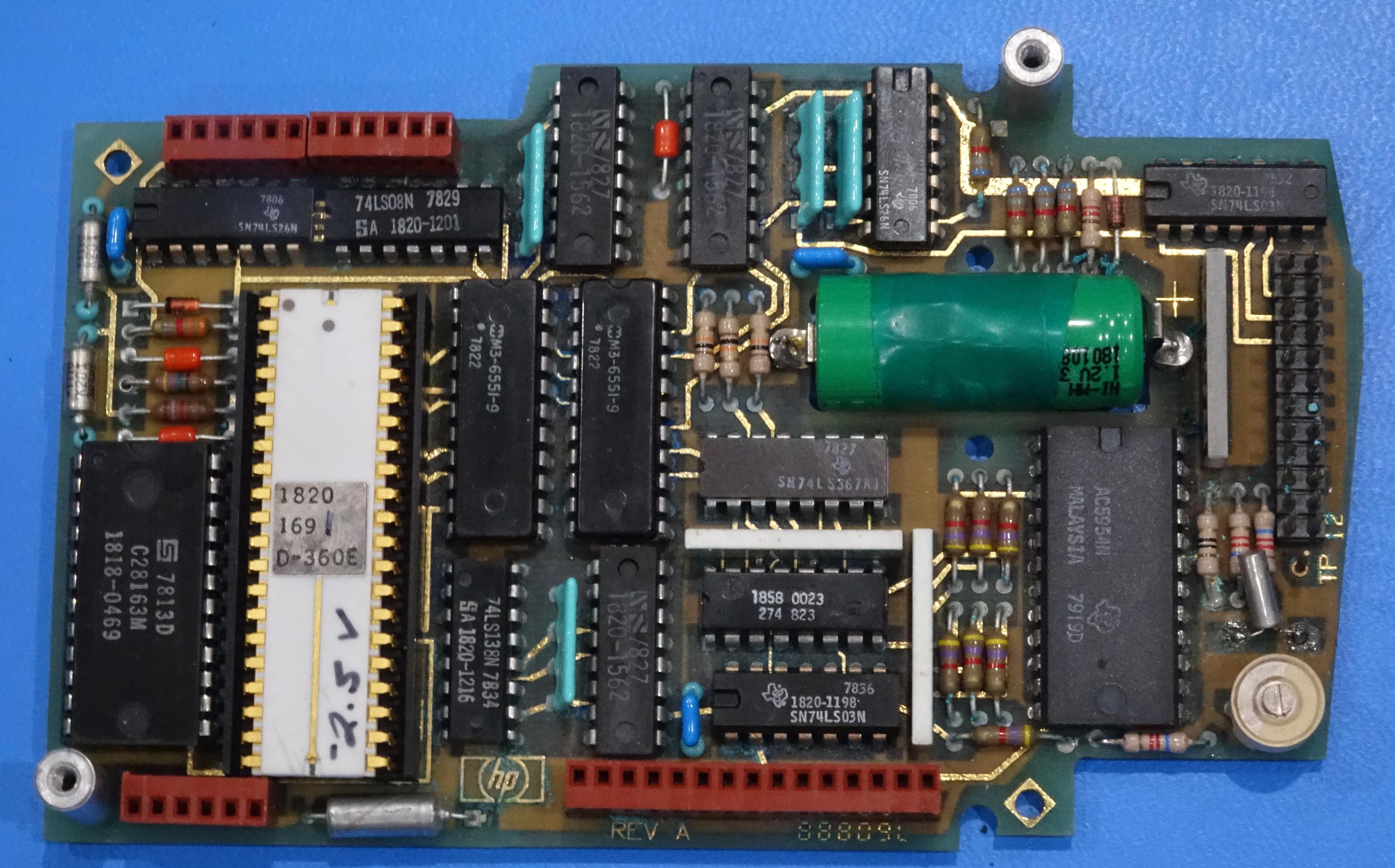
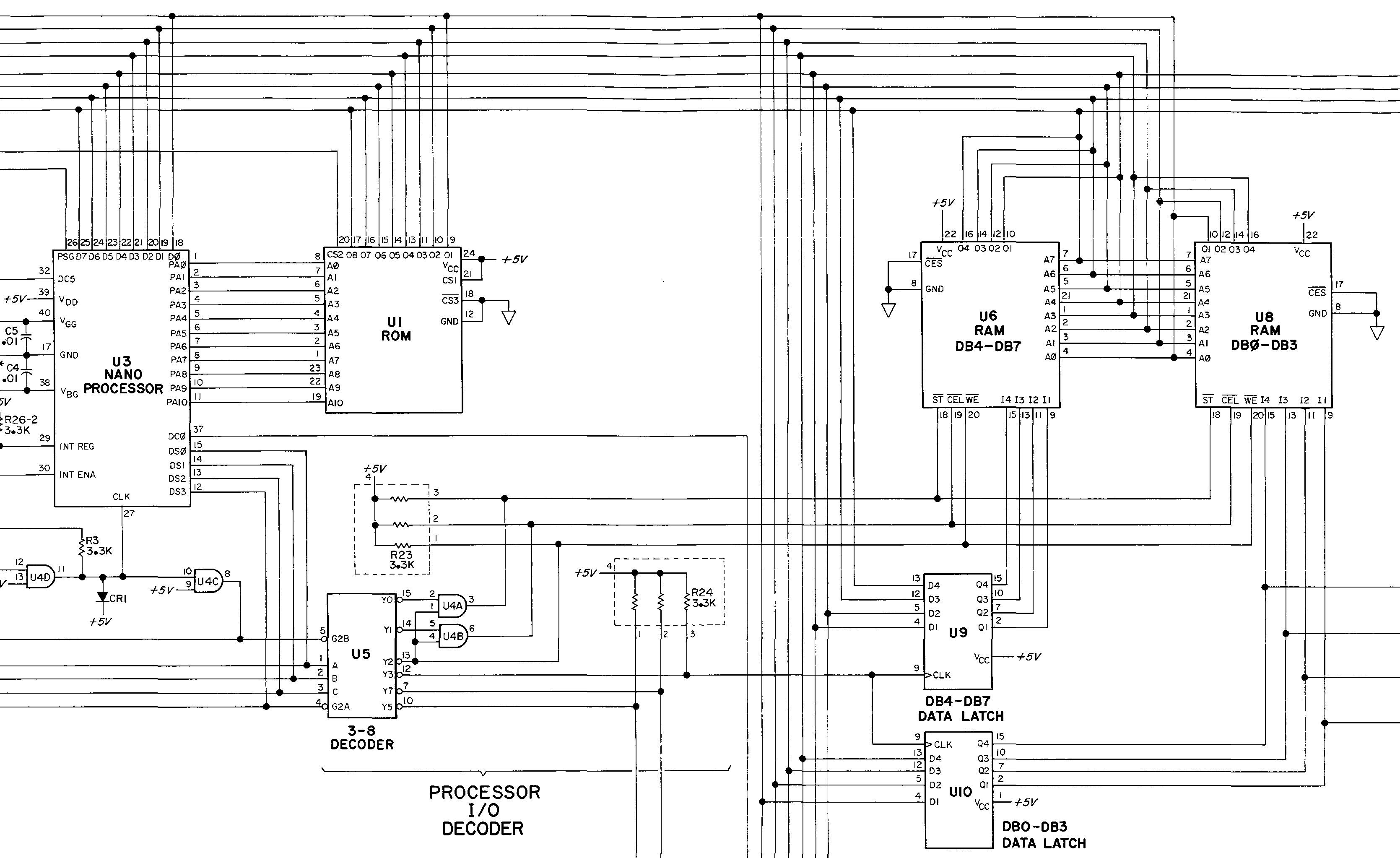
  19. The clock board schematic shows how the two 256×4 RAM chips are connected to the Nanoprocessor. The Nanoprocessor’s I/O port select pins are connected to the “3-8 Decoder” U5, which produces a separate signal for each I/O port. Three of these signals go to the RAM chip’s control pins, while one signal controls the Data Latch chips U9 and U10 that hold write data.
    RAM chips connected to the Nanoprocessor. From the Clock service manual.


    All I/O ports use the Nanoprocessor’s data bus (top) for communication, so the data bus is connected to both the address and data pins of the RAM chips. For a read, the RAM address is written to the RAM chips via one I/O port and then the data is read from RAM via a second port. In both cases, the values go across the data bus, while the signal from the “3-8 Decoder” indicates what to do with the values. For a write, the first I/O operation stores the byte value in the latches, and then the second I/O operation sends the address to the RAM chips. While this may seem like a clunky, Rube-Goldberg approach, it works well in practice; a read or write can be done with two bytes of instructions.

    (Many processors, such as the 6502, used memory-mapped I/O; I/O devices were mapped into the memory address space and accessed through memory read/write operations. The Nanoprocessor is the opposite, putting RAM into the I/O port space and accessing it through I/O operations.)

    Adding an ALU uses a similar approach, as in the HP 3455A voltmeter (schematic), which contains two Nanoprocessors. The voltmeter uses two 74LS181 ALU chips to implement an 8-bit ALU that it uses to scale value and compute percentage error. Two output ports provide the arguments and another port specifies the operation. The 8-bit result is read from a port, while the processor reads the carry through a GPIO pin. (At this point, I’d wonder if it wouldn’t be better to use a processor that includes arithmetic.) 


PCI Express in Depth – Transaction Layer

PCI Express in Depth – Transaction Layer
by Luigi Filho on 09-06-2020 at 7:00 am

PCI Express in Depth Transaction Layer

In the last article i write about the Data Link Layer, in this article i’ll write about the Transaction Layer.

This layer’s primary responsibility is to create PCI Express request and completion transactions. It has both transmit functions for outgoing transactions, and receive functions for incoming transactions.

The Transaction Layer uses TLPs to communicate request and completion data with other PCI Express devices. TLPs may address several address spaces and have a variety of purposes. Each TLP has a header associated with it to identify the type of transaction.

I’ll explain two main things, the Transaction Layer Packet (TLP) and the TLP Handling

Transaction Layer Packet

An generic TLP is show in the figure below:

A TLP consists of a header, an optional data payload, and an optional TLP digest. The Transaction Layer generates outgoing TLPs based on the information it receives from its device core. The Transaction Layer then passes the TLP on to its Data Link Layer for further processing. The Transaction Layer also accepts incoming TLPs from its Data Link Layer.

TLP Headers

All TLPs consist of a header that contains the basic identifying information for the transaction. The TLP header may be either 3 or 4 DWords in length, depending on the type of transaction.

The format of first DWord is shown in the figure below

To the article don’t get much extensive, i’ll not cover each bit, but if you like, leave a comment with this request and then i’ll cover bit by bit

TLP Data Payload

Whether or not a TLP contains a data payload depends on the type of packet. If present, the data payload is DWord-aligned for both the first and last DWord of data.

The data payload for a TLP must not exceed the maximum allowable payload size, as defined in the device’s control register (and more specifically, the Max_Payload_Size field of that register).

TLP Digest

The Data Link Layer provides the basic data reliability mechanism within PCI Express via the use of a 32-bit LCRC. This LCRC code can detect errors in TLPs on a link-by-link basis and allows for a retransmit mechanism for error recovery.

To ensure end-to-end data integrity, the TLP may contain a digest that has an end-to-end CRC. This optional field protects the contents of the TLP through the entire system, and can be used in systems that require high data reliability. The Transaction Layer of the source component generates the 32-bit ECRC.

TLP Handling

A TLP that makes it through the Data Link Layer has been verified to have traversed the link properly, but that does not necessarily mean that the TLP is correct. A TLP may make it across the link intact, but may have been improperly formed by its originator. As such, the receiver side of the Transaction Layer performs some checks on the TLP to make sure it has followed the rules. If the incoming TLP does not check out properly, it is considered a malformed packet, is discarded (without updating receiver flow control information) and generates an error condition. If the TLP is legitimate, the Transaction Layer updates its flow control tracking and continues to process the packet

An flowchart is shown below 

Request Handling

If the TLP is a request packet, the Transaction Layer first checks to make sure that the request type is supported. If it is not supported, it generates a non-fatal error and notifies the root complex.

I’ll not get into details, but an flowchart is show below of this process.

Completion Handling

If a device receives a completion that does not correspond to any outstanding request, that completion is referred to as an unexpected completion. Receipt of an unexpected completion causes the completion to be discarded and results in an error-condition (nonfatal).

The receipt of unsuccessful completion packets generates an error condition that is dependent on the completion status. The details for how successful completions are handled and impact flow control logic i’ll not cover because this article is getting too big.

But as always, if you want me to cover, leave a comment.

Remember that this series was suggested by a reader.

With this post i’ll end the PCIe in Depth series, if you lost some article, you can check the first, the physical layer and data-link layer.


PCI Express in Depth – Data Link Layer

PCI Express in Depth – Data Link Layer
by Luigi Filho on 09-06-2020 at 6:00 am

PCI Express in Depth Data Link Layer

In the last article, i wrote about the physical layer, now let’s take a look in the next layer the data link layer.

The Data Link Layer serves as the “gatekeeper” for each individual link within a PCI Express system. It ensures that the data being sent back and forth across the link is correct and received in the same order it was sent out. The Data Link Layer makes sure that each packet makes it across the link, and makes it across intact.

The Data Link Layer adds a sequence number to the front of the packet and an LCRC error checker to the tail. Once the transmit side of the Data Link Layer has applied these to the TLP, the Data Link Layer forwards it on to the Physical Layer.

For incoming TLPs, the Data Link Layer accepts the packets from the Physical Layer and checks the sequence number and LCRC to make sure the packet is correct. If it is correct, the Data Link Layer removes the sequence number and LCRC, then passes the packet up to the receiver side of the Transaction Layer.

Now let’s talk about theses TLP’s.

The TLP stands for Transaction Layer Packet (TLP) and in the figure below is show a typical packet:

Now there is two main things we need to know:

  • Sequence Number – The Data Link Layer assigns a 12-bit sequence number to each TLP as it is passed from the transmit side of its Transaction Layer. The Data Link Layer applies the sequence number, along with a 4-bit reserved field to the front of the TLP.
  • LCRC – The Data Link Layer protects the contents of the TLP by using a 32-bit LCRC value. The Data Link Layer calculates the LCRC value based on the TLP received from the Transaction Layer and the sequence number it has just applied. On the receiver side, the first step that the Data Link Layer takes is to check the LCRC value. It does this by applying the same LCRC algorithm to the received TLP (not including the attached 32-bit LCRC).

The data link have three more concepts that you need to be aware of:

  • Retries – The transmitter cannot assume that a transaction has been properly received until it gets a proper acknowledgement back from the receiver. If the receiver sends back a Nak (for something like a bad sequence num- ber or LCRC), or fails to send back an Ack in an appropriate amount of time, the transmitter needs to retry all unacknowledged TLPs. To accomplish this, the transmitter implements a Data Link Layer retry buffer
  • Data Link Layer Packets (DLLPs) – DLLPs support link operations and are strictly associated with that given link. DLLPs always originate at the Data Link Layer and are differentiated from TLPs when passed between the Data Link Layer and Physical Layer. Additionally, TLPs have an originator and destination that are not necessarily link mates, while a DLLP is always intended for the device on the other side of the link. DLLPs have four major functions (types): Ack DLLP, Nak DLLP, FC DLLPs(Flow Control DLLPs) and PM DLLPs (Power Management DLLPs).
  • Data Link Layer Control – The Data Link Layer tracks the state of the link and communicates this status with both the Transaction and the Physical Layer. The Data Link Layer keeps track of the link status via a state machine with the following parameters: States (DL_Inactive, DL_Init and DL_Active) Status Outputs (DL_Down and DL_Up)

Basically the Data-Link Layer will process the sequence number and the LCRC.

If you have any question, leave in the comment section below.

If you want make a request, leave in the comment, this article was a request.

You can check the first and last article about PCIe hereand here.


Alchip at TSMC OIP – Reticle Size Design and Chiplet Capabilities

Alchip at TSMC OIP – Reticle Size Design and Chiplet Capabilities
by Mike Gianfagna on 09-04-2020 at 10:00 am

Alchip machine learning design

This is another installment covering TSMC’s very popular Open Innovation Platform event (OIP), held on August 25. This event presents a diverse and high-impact series of presentations describing how TSMC’s vast ecosystem collaborates with each other and with TSMC.  This presentation is from Alchip, presented by James Huang, Alchip’s vice president of R&D. You may recall a post I did recently that detailed Alchip’s work in supercomputer processor design. In that post, I described Alchip’s accomplishments as “a tour de force of technology, with many advanced design and packaging accomplishments.” Well, they’re at it again. This time presenting the details of a reticle size design and chiplet capabilities.

The design presented is a machine learning application fabricated in TSMC’s 12nm process. It consists of four die on an organic substrate (8/2/8). The package is an MCM FFCBGA (85 X 85) with 6,456 balls. The four-die system consumes 520 watts and is pictured above. By now, you should start to have a headache thinking about this design. I did. To complete the picture, each chip is a reticle size monster with 1.6B gates, 180MB of SRÅM and 204GB/s of memory bandwidth. Die-to-die communication is accomplished with an APLink 1.0 PHY. This design is truly a record-setting achievement, delivering 21.11 GFLOPS/watt.

Back to my headache. It got worse as James described the design challenges Alchip faced with this design. Soc design challenges include:

  • >1B gate count and multiple level logical/physical hierarchy
  • >100M on-chip SRAM and yield considerations
  • Thousands of repeated cores and data bus traffic
  • Extremely high static/dynamic power consumption and low power design
  • Clock network design and power distribution network design
  • DFT and testing strategy considering redundancy

For the package, design challenges include:

  • Die-to-die interconnection on substrate
  • PCB/package/SoC co-design
  • Thermal considerations
  • Warpage with 85x85mm² package size

Your head really has to be hurting at this point. So, how does one implement a design of this extreme complexity and size? Alchip packed a lot of innovation into the design process. James outlined some of the approaches. At the physical level, a channel-less floorplan with symmetry was used. The clocking strategy included chip-level clock phase control with a fishbone architecture. Power consumption was managed with adaptive voltage scaling, dynamic voltage and frequency scaling, clock and power gating, dual-rail SRAMs and a customized data path. In other words, just about every trick in the book, which is required to deliver reticle size designs and chiplet capabilities.

For DFT, an abutment design approach was used and custom DFT strategies were implemented for critical and non-critical logic.  A redundancy and repair capability was also included.  For testing and repair, the failure map was recorded in eFuse and the smart repair strategy considered scan and MBIST failures together.

Communication between the four dies is through the organic substrate as shown in the figure below. The APLink 1.0 PHY delivers 576Gbps per die-to-die channel in the N12 process. Multiple Tbps are possible in N7 and N5 and an APLink 3.0 design for 5nm technology is under development. The approach supports TSMC’s CoWoS and InFO packaging.

For signal integrity, 2.5D/3D model extraction was employed for high-speed signals and power-aware SPICE simulation accounted for noise induced effects. Power integrity required a lot of focus as each die draws over 150 amps of average current, with peak-to-peak variation greater than 40% of the average.

Given the high power of this design, electrical-thermal co-design was used and Alchip collaborated closely with the customer to model the cooling system. Mechanical samples were verified ahead of production to ensure warpage of the large interposer wouldn’t impact assembly yield.

This presentation was very impressive, and this design sets a new bar in complexity and power management. You can learn more about this reticle size design and its chiplet capabilities from Alchip’s press release.

Also Read:

Alchip moves from TSMC 7nm to 5nm!

Alchip Delivers Cutting Edge Design Support for Supercomputer Processor

CEO Interview: Johnny Shen of Alchip


Highlights of the TSMC Technology Symposium – Part 1

Highlights of the TSMC Technology Symposium – Part 1
by Tom Dillinger on 09-04-2020 at 8:00 am

A72 core high density

Recently, TSMC held their 26th annual Technology Symposium, which was conducted virtually for the first time.  This article is the first of three that attempts to summarize the highlights of the presentations.

This article focuses on the TSMC process technology roadmap, as described by the following executives:

  • Y.J. Mii, SVP, R&D:  “Advanced Technology Leadership”
  • Kevin Zhang, SVP, Business Development:  “Specialty Technology Leadership”
  • Y.P. Chin, SVP, Operations:  “Manufacturing Excellence”

Key Takeaways

  • The N7 to N5 to N3 process node cadence continues on an aggressive schedule, with each transition offering a full-node areal scaling.
  • N3 will utilize a traditional FinFET device architecture.
  • The new node N12e introduces an ultra-low power offering  – the cell library VDD is reduced to 0.4V.
  • The availability of alternative non-volatile memory technologies (RRAM, MRAM) offers continued scaling of applications requiring embedded NVM memory (eFlash).  The availability of (high-endurance, SRAM-like) MRAM provides very interesting memory cache system design opportunities.
  • TSMC is planning a huge R&D investment for technology development past N3.

N7, N5, and N3 Roadmap

N7 entered high volume manufacturing (HVM) in 2018, at Fab 15.  TSMC provided a forecast for more than 200 N7/N7+ new tapeouts (NTOs) in 2020.

Recall that the initial N7 process definition did not incorporate EUV lithography – the subsequent N7+ process added EUV as a replacement for a few critical-dimension layers.   Node N6 will offer a logic density boost (~18%) over N7, using a block-level physical re-implementation flow with a new Foundation IP library – e.g., mask layer reduction, CPODE cell abutment.

The next node, N5, entered HVM in 2Q2020, at Fab 18 in Tainan.  EUV lithography has been applied extensively.   (Fab 18 broke ground in January, 2018, with equipment move-in a year later – this is an extremely impressive ramp from fab construction to HVM, especially with EUV litho.)

A future N5+ variant will provide a ~5% performance boost, with HVM in 2021.  Node N4 is a mid-life kicker to N5, with a mask layer cost reduction (while maintaining design rule capability to existing N5 IP).  Risk production for N4 is 4Q21, with HVM in 2022.

N3 is well-defined, with EDA vendors already providing design enablement flows and with IP in active development – risk production is planned for 2021, with HVM in 2H22.

TSMC provided two charts to illustrate the PPA comparisons between these nodes.  The first depicts the comparisons for an Arm A72 core.  Recall that TSMC has focused their Foundation IP development and EDA enablement for different platforms – the comparison below utilizes the high-density based physical implementation flow associated with the Mobile and IoT platforms.

The high-performance platform (HPC) comparison for N7, N5, and N3 is shown below, using the physical implementation of the Arm A78 core as the reference.

The way to interpret these curves is that a horizontal line represents the performance gain at iso-power, which the vertical line depicts the power gains at iso-performance.

In both cases, the N7 to N5 and N5 to N3 transitions incorporate a full-node areal density increase, although it should be noted that the SRAM IP and analog density scaling factors are less.

N12e

The IoT and mobile platforms are driven by the need for ultra-low power dissipation, achieved through supply voltage reduction and the availability of ultra-low leakage (ULL, high Vt) devices.  Additionally, an ultra-low leakage SRAM bit cell offering is needed.  Also, a new class of applications – AIoT, or Artificial Intelligence of Things – is emerging for the edge-centric, ultra-low power market.

TSMC introduced a new process designation, N12e, specifically to address these requirements – working from the N12FFC+ baseline, N12e is currently in risk production status.  The N12e offering includes several key characteristics:

  • cell library IP operating at VDD = 0.4V
  • significant focus on statistical process control, to minimize device variation
  • 0.5X power (@ iso-performance) compared to N22ULL
  • 1.5X performance (@ iso-power) compared to N22ULL

The application of VDD=0.4V necessitates focus on the EDA flows for delay calculation/static timing analysis and coupled noise electrical analysis – the status of the EDA enablement for N12e will be covered in a subsequent article.   (Please refer to:  http://n12e.tsmc.com.)

RF Roadmap

To support the rapidly growing 5G market, TSMC has maintained focus on RF CMOS process development, striving for enhanced device characteristics.  The current RF offerings are based on the N28HPC and N16FFC processes.

The new RF roadmap introduced N6RF, with significantly improved power and device noise factor (NF, @5.8GHz) over current devices.   Design kit enablement for N6RF will be released in 2Q21.

Non-volatile memory (NVM) Roadmap – eFlash, RRAM, and MRAM

TSMC’s current embedded flash memory IP for the N28HPC (HKMG) node is being qualified for the automotive design platform (i.e., endurance cycles and data retention at 150C) – target date is end of 2020.

For process nodes after N28, scaling of floating gate-based flash memory becomes more difficult (expensive).  The NVM roadmap transitions to Resistive (filamentary) RAM, with N22 tapeouts this year (at 125C, non-automotive grade).  Magneto-resistive RAM (MRAM) is also available for N22 tapeouts, with automotive grade qualification in 4Q20.  Further, N16 MRAM IP will be available for risk production in 4Q21.

Initially, RRAM and MRAM technologies will be used as IP replacing eFlash applications – e.g., 10K+ endurance cycles.  TSMC indicated an “SRAM-like” MRAM IP offering for N16 will be available in 4Q22 – clearly, significant focus is being applied to increase MRAM endurance.  MRAM as a non-volatile, high-density L3/L4 SRAM-replacement memory cache will offer some very unique system architecture design opportunities.

Advanced process node fab capacity

To support the demand for nodes N16 to N5, 300mm wafer Gigafab capacity has experienced a CAGR of 28% from 2016 to 2020.  The fab capacity for N7 alone has grown 3.5X in just over two years, from 2018 to 2020.  Additionally, the capacity for N5 is planned for 3X growth from today to 2022.

Y.P. Chin highlighted that EUV learning from N7+ and N5 has enabled an extremely aggressive improvement in defect density (D0).  For example, refer to the innovation that TSMC has deployed for EUV mask cleaning:  link.

There are also major expansion plans for the Advanced Packaging line facilities in Tainan.

R&D Investment

A consistent theme through the presentations was the extensive investment TSMC is making in future technology R&D.   Specifically, TSMC is building a new R&D Center in Hsinchu, as depicted below.  The goal will be to enable “thousands of engineers” to work on new transistor architectures, materials, and process flows required for the nodes after N3, and “for the next twenty years” – more on these initiatives shortly.

Construction of the R&D center got underway in 1Q20, with occupancy starting in 2021.

Adjacent to the new R&D center, TSMC illustrated new fab construction in Hsinchu specifically designated for the “N2” process node.  Like the other TSMC Gigafabs – e.g., Fab 12, Fab 15, Fab 18, — the N2 fab construction will evolve in multiple phases.

The planned investment in R&D and fab deployment for “N2 and beyond” is definitely impressive.

Future Technology R&D

TSMC provided a glimpse into some of the future technologies currently being investigated, as the R&D activity continues to ramp.

  • RC enhancements

FinFET devices offer significant benefits in areal drive current and subthreshold leakage electrostatic channel control over planar devices – yet, one of the disadvantages is the additional Cgs and Cgd parasitic capacitance from the gate traversal over the fin(s) and the raised source/drain plus M0 metallization.  TSMC will be introducing an air-gap process in the dielectric between gate and source/drain to reduce these parasitics.

Additionally, interconnect R*C delays will be improved with the introduction of a new via trench barrier process.

  • EUV litho development

To enable aggressive lithography scaling for pitches less than 80nm using 193i illumination, TSMC introduced mask data decomposition (“coloring”) at the N20 node.  Double and quad multipatterning (SADP or 2P2E, and SAQP) have enabled further scaling.   Inverse lithography technology (ILT) algorithms, as part of a source-mask optimization (SMO) mask data preparation methodology, was also deployed.   13.5nm EUV lithography was introduced for N7+, as mentioned above.  To enable further scaling, EUV multipatterning (2P2E) is required.

TSMC showed lithographic patterning/etch in support of an 18nm interconnect pitch.

  • high NA EUV

The numerical aperture of a lithography system defines the resolution capability, a function of the cone of light captured  and the refractive index of the entire lens system.  The resolution is inversely proportional to the NA.  TSMC is working closely with ASML on the next generation of “high NA” EUV equipment and corresponding resist technology, to enable finer resolution in future nodes.

  • GAA nanosheets

TSMC highlighted their R&D efforts to implement gate all-around nanosheets, as a FinFET replacement.

The N3 process definition starts with a conventional FinFET device.  (To achieve increased performance and fin pitch, the fin height and aspect ratio for N3 will need to be improved.)

As has been the case for TSMC node transitions, adhering to the roadmap schedule has been a paramount priority.  Y.J. Mii said, “After carefully evaluating customer needs and technology maturity, N3 continues to use FinFET devices.  Our R&D team has extensive experience with nanowire and nanosheet technology, and have demonstrated 32Mb SRAM testsite yield.  We will have the technology options for each new node ready in advance – the right technology at the right time.”  It will be interesting to see how GAA device architectures evolve.

  • unique “2D” device semiconducting channel material

TSMC referred to a technical paper published earlier this year, showing promising results for a replacement to the Si (or SiGe) FinFET device.  Semiconducting “monolayers” of MoS2 serve as the (planar) field-effect device channel, offering improved carrier mobility.  (Reference:  A.S. Chou, et al., VLSI Symposium 2020).

The figure below illustrates a single monolayer of MoS2, the HfO2 gate dielectric, and either a (large area) Si or a local Pt “back gate” device structure.  The device drive current and Ion/Ioff ratio shows great promise – reducing the contact resistance (Rc) from the S/D metal to the semiconducting layer is a key process development challenge.

  • carbon nanotubes

TSMC also referred to a recently published paper illustrating the implementation of a deposited layer of carbon nanotubes (CNT) for a unique application.  The nanotubes were incorporated as part of the (low temperature-restricted) back-end-of-line flow in N28, with patterning of gate and source/drain metallization.  The specific application for which these devices are targeted is for the logic circuit power-gating “header”.  (Reference:  Cheng, et al, IEDM, 2019, paper 19.2)

Current power-gating implementations utilize multiple silicon devices (low R) connected between the “always on” and switched power rails connected to the block logic.  These designs require unique block-level physical design, specific cell library images, and modified (global/local) power distribution networks, adversely impacting areal circuit density and routability.  A semiconducting CNT power gating circuit could offer a significant PPA boost – ongoing focus on reducing the overall series “on” resistance will be key.

As an aside, it is perhaps unwise to read too much into the R&D part of the Symposium presentations, in terms of what was and was not mentioned for post-N3 architectures.  Nevertheless, the following options being widely investigated within the semiconductor industry were not discussed:  negative-capacitance FETs (NC-FETs, integrating ferroelectric materials), vertical nanowires (VNW), tunnel FETs, or N3XT (“full 3D” die integration of logic, memory, and NVM).

Look for subsequent articles highlighting TSMC packaging technology and design enablement presentations to follow.

-chipguy

Highlights of the TSMC Technology Symposium – Part 2

Highlights of the TSMC Technology Symposium – Part 3


How an Nvidia/ARM deal could create the dominant ecosystem for the next computer era

How an Nvidia/ARM deal could create the dominant ecosystem for the next computer era
by Michael Bruck on 09-04-2020 at 6:00 am

PC operating profits

Over the past few weeks, there have been numerous reports about Nvidia’s overtures to acquire Arm. The news has mostly been obsessed about the $31 billion that Arm’s current owner, Softbank, paid for Arm and whether Nvidia could pay such an eye-watering price to buy this asset. There is also pushback from Herman Hauser who was one of Arm’s earliest backers, raising concerns that Arm’s destiny is vital for Britain’s future, which is an odd concern given that Softbank is a Japanese company. Putting all this aside for a moment, I would like to focus on the strategic importance of such a merger and, if the merger does go through, why this could result in a momentous change in the balance of power in the computer and semiconductor industry and why a combined Nvidia and Arm could truly be a game-changer.

The next strategic inflection point in computing will be the cloud expanding to the edge, involving highly parallel computer architectures connected to hundreds of billions of IoT devices. Nvidia is uniquely positioned to dominate that ecosystem, and if it does indeed acquire ARM within the next few weeks as expected, full control of the ARM architecture will virtually guarantee its dominance.

Every 15 years, the computer industry goes through a strategic inflection point, or as Jefferies US semiconductors analyst Mark Lipacis calls it, a tectonic shift, that dramatically transforms the computing model and realigns the leadership of the industry. In the ’70s the industry shifted from mainframe computers, in which IBM was the dominant company, to minicomputers, which DEC (Digital Equipment Corporation) dominated. In the mid-’80s the tectonic shift was PCs, where Intel and Microsoft defined and controlled the ecosystem. Around the turn of the millennium, the industry shifted again to a cell phone and cloud computing model; Apple, Samsung, TSMC, and ARM benefited the most on the phone side, while Intel remained the major beneficiary of the move to cloud data centers. As the chart below shows, Intel and Microsoft (a.k.a. “Wintel”) were able to extract the majority of the operating profits in the PC era.

Source: Jefferies, company data

According to research from investment bank Jefferies, in each previous ecosystem, the dominant players have accounted for 80% of the profits. For example, Wintel in the PC era and Apple in the smartphone era. These ecosystems did not happen by accident and are the result of a multi-pronged strategy by each company that dominated its respective era. Intel invested vast sums of money and resources into developer support programs, large developer conferences, software technologies, VC investments through Intel Capital, marketing support, and more. The result of the Wintel duopoly can be seen in the chart above. Apple has done much the same, with its annual developer conference, development tools, and financial incentives. In the case of the iPhone, the App Store has played an additional role, making the product so successful, in fact, that it is now the target of complaints by the developers who played a key role in cementing Apple’s dominance of the smartphone ecosystem. The chart below shows how Apple has the lion’s share of the operating profits in mobile phones.

Source: Jefferies, company data

Intel maintained dominance of the data center market for decades, but that dominance is now under threat for several reasons. One is that the type of software workload mobile devices generate is changing. The vast amounts of data these phones generate requires a more parallel computational approach, and Intel’s CPUs are designed for single-threaded applications. Starting 10 years ago, Nvidia adapted its GPU (graphics processing unit) architecture (originally designed as a graphics accelerator for 3D games) into a more general-purpose parallel processing engine. Another reason Intel is under threat is that the much larger volume of chips sold in the phone market has given TSMC a competitive advantage, since TSMC was able to take advantage of the learning curve to get ahead of Intel in process technology. Intel’s 7nm process node is now over a year behind schedule. Meanwhile, TSMC has shipped over a billion chips on its 7nm process, is getting good yields on 5nm, and is sampling 3nm parts. Nvidia, AMD, and other Intel competitors  are all manufacturing their chips at TSMC, which gives them a major competitive advantage.

Nvidia’s domain

Parallel computing concepts are not new and have been part of computer science for decades, but they were originally relegated to highly specialized tasks such as using supercomputers to simulate nuclear bombs or weather forecasting. Programming parallel processing software was very difficult. This all changed with the CUDA software platform that Nvidia launched 13 years ago and which is now on its 11th generation. Nvidia’s proprietary CUDA software platform lets developers leverage the parallel architecture of Nvidia’s GPUs for a wide range of tasks. Nvidia also seeded computer science departments at universities with GPUs and CUDA, and over many iterative improvements the technology has evolved into the leading platform for parallel computing at scale. This has caused a tectonic shift in the AI industry — moving it from a “knowledge-based” to “data-based” discipline, which we see in the growing number of AI-powered applications. When you say “Alexa” or “Hey Siri,” the speech recognition is being processed and interpreted by a parallel processing software algorithm most likely powered by an Nvidia GPU.

A leading indicator for computer architecture usage is Cloud Data Instances. The number of these instances represents the usage demand for applications in the leading CSPs (cloud service providers), such as Amazon AWS, Google Cloud Platform, Microsoft Azure, and Alibaba Cloud. The top four CSPs are showing that Intel’s CPU market share is staying flat to down, with AMD growing quickly, and ARM with Graviton getting some traction. What is very telling is that demand for dedicated accelerators is very strong and being dominated by Nvidia.

Source: Jefferies, company data

Nearly half of Nvidia’s sales revenues are now driven by data centers, as the chart above shows. As of June this year, Nvidia’s dedicated accelerator share in cloud data instances is 87%. Nvidia’s accelerators have accounted for most of the data center processor revenue growth for the past year.

The company has created a hardware-software ecosystem comparable to Wintel, but in accelerators. It has reaped the rewards of the superior performance of its architecture and of creating the highly popular CUDA software platform, with a sophisticated and highly competitive developer tools and ecosystem support program, a highly attended annual GPU Technology Conference, and even an active investment program, Inception GPU Ventures.

Where ARM comes in

But Nvidia has one competitive barrier remaining that prevents it from complete domination of the data center ecosystem: It has to interoperate within the Wintel ecosystem because the CPU architecture in data centers is still x86, whether from Intel or AMD.

ARM’s server chips market share is still minute, but it has been extremely successful. And, with TSMC as a manufacturing partner, it is rapidly overtaking Intel in raw performance in market segments outside of mobile phones. But ARM’s weakness is that the hardware-software ecosystem is fragmented, with Apple and Amazon having a mostly proprietary software approach and smaller companies such as Ampere and Cavium being too small to create a large industry ecosystem comparable to Wintel.

Nvidia and ARM announced in June that they will work together to make ARM CPUs work with Nvidia accelerators. First of all, this collaboration gives Nvidia the ability to add computing capabilities to its data center business. Secondly, and more importantly, it puts Nvidia in a strong position to create a hardware-software ecosystem around ARM that would be a serious threat to Intel.

The coming shift

The reason such a partnership is particularly important today is because the computer industry is going through its next strategic inflection point. This new tectonic shift will have major repercussions for the industry and the competitive landscape. And if historical trends continue, a merged Nvidia/ARM would result in a market at least 10 times larger than today’s mobile phone or cloud computing market. It is an understatement to say that the stakes are huge.

There are several forces driving this new shift. One is the emergence of faster 5G networks that are designed to support a far larger number of devices. One of the key features of 5G networks is edge computing, which will put high-performance computing right at the very edge of the network, one hop away from the end-device. Today’s mobile phones are still tied to a descendant of the old client-server architecture established in the ’90s with networked PCs. That legacy results in high latency networks, which is why we experience those annoying delays on video calls.

Next-generation networks will have high-performance computers with parallel accelerators at the very edge of the network. The endpoints — including autonomous vehicles, industrial robots, 3D or holographic communications, and smart sensors everywhere — will require a much tighter integration with new protocols and software architectures. This will achieve much faster, and extremely low latency communications through a distributed computing architecture model. The amounts of data produced — and needing processing — will increase by orders of magnitude, driving demand for parallel computing even further.

Nvidia’s roadmap

Nvidia has already made its intentions clear that cloud-to-edge computing is on its roadmap:

“AI is erupting at the edge. AI and cloud native applications, IoT and its billions of sensors, and 5G networking now make large-scale AI at the edge possible. But it needs a scalable, accelerated platform that can drive decisions in real time and allow every industry to deliver automated intelligence to the point of action — stores, manufacturing, hospitals, smart cities. That brings people, businesses, and accelerated services together, and that makes the world a smaller, more connected place.”

Last year Nvidia also announced that it is working with Microsoft to collaborate on the Intelligent Edge.

This is why it makes strategic sense for Nvidia to buy ARM and why it would pay a very high price to be able to own this technology. Ownership of ARM would give Nvidia greater control over every aspect of its ecosystem with far greater control of its destiny. It would also eliminate Nvidia’s dependence on the Intel compute stack ecosystem, which would greatly increase its competitive position. By owning ARM instead of just licensing it, Nvidia could add special instructions to create even tighter integration with its GPUs. To get the highest performance, one needs to integrate the CPU and GPU on one chip, and since Intel is developing its competing Xe line of accelerators, Nvidia needs to have its own CPU.

Today Nvidia leads in highly parallel compute and Intel is trying to play catch-up with its Xe lineup. But as we have learned from the PC Wintel days, the company that controls the ecosystem has a tremendous strategic advantage, and Nvidia is executing well to position it to become the company that will be the dominant player in the next era of computing. Nvidia has a proven track record of creating an impressive ecosystem around its GPUs, which puts it in a very competitive position to create a complete ecosystem for edge computing including the CPU.

Michael Bruck is a Partner at Sparq Capital. He previously worked at Intel, where he was Chief of Staff to the then CEO, Andy Grove, before heading Intel’s business in China.


World’s Leading Chip Designers at IDEAS Digital Forum Show How to Streamline Design Flows and Reduce Design Cost

World’s Leading Chip Designers at IDEAS Digital Forum Show How to Streamline Design Flows and Reduce Design Cost
by Daniel Nenni on 09-03-2020 at 10:00 am

ANSYS IDEAS Airplane

Innovative Designs Enabled by Ansys Semiconductor

I’m excited to announce that general registration is now open for the new Ansys IDEAS Digital Forum!  IDEAS, hosted by Ansys Semiconductor, is a virtual gathering of top industry executives, thought leaders, and designers from some of the biggest IP, chip design, semiconductor foundry and electronic system companies in the world. Log in to IDEAS to join with your peers to listen to industry leaders and technical experts discuss the semiconductor industry. And then ask them questions in live Q&A sessions.

Design automation and multiphysics simulation tools are key leverage points in your production flow where you have options available to not only reduce your risk profile but also influence the bottom line by reducing costs, improving product quality, and speeding time to market.  IDEAS is an opportunity for you to stay on top of what is going on in the electronic design market with Keynote presentations from senior industry executives including:

  • Len Orlando III Air Force Research Laboratory Sensors Directorate, Wright Patterson AFB
  • Prith Banerjee CTO, Ansys
  • Rob Aitken R&D Fellow, ARM
  • Vicki Mitchell & Rob Harrison VP of Engineering & Sr. Director at ARM
  • Dhiraj Mallick VP of Engineering at Cerebras Systems
  • Eric Ladizinsky Co-Founder and Sr. Scientist at D-Wave Systems
  • Mallik Tatipamula CTO of Ericsson SV
  • Subhasish Mitra of Electrical Engineering and Computer Science, Stanford University
  • Suk Lee Sr. Director of Design Infrastructure Marketing at TSMC

These distinguished, high profile executives will be sharing their insights on technology and business trends from multiple perspectives and will be taking live questions from audience members attending IDEAS.

The theme of IDEAS Digital Forum focuses on how multiphysics simulation is accelerating the twin industry trends of Moore and Beyond Moore. Moore’s Law is racing towards ever smaller silicon process geometries, with 3nm now on the horizon. This enables huge ICs to be designed for AI/ML applications, high-performance computing, and 5G. But the expense of designing at the leading edge is also rising and a second evolutionary path has emerged called Beyond Moore, or More Than Moore,  that pushes a parallel evolutionary track based on a multi-die approach to system integration with technologies like 3DIC, wafer-scale integration, and a disaggregation of SoCs into discrete chiplets for applications ranging from intelligent sensors, autonomous, and edge-node compute.  It is a fascinating time to be in semiconductors with these complex market and technology forces creating many opportunities and tradeoffs on which approach to pick, based on your end application.

The afternoons of both days at IDEAS are taken up with technical Breakout Sessions featuring over 30 speakers from companies including:

Intel Nvidia Qualcomm
Broadcom MediaTek ST Microelectronics
Samsung Alphawave Synaptics
Google HP Enterprise Xilinx

These sessions will focus on practical design experiences for applications in the areas of 3D-IC electrothermal analysis, electromagnetic coupling, the timing impact of voltage drop, RTL power analysis, and power integrity signoff.  Here too, virtual attendees logged in to IDEAS will be able to submit questions to the authors in real time and get immediate answers.

For a broader perspective, the Multiphysics Solutions track will feature experts on industry-wide technology challenges including 5G communications, autonomous vehicles, designing in the cloud, and design for  reliability. They will highlight how electronic design is impacted by these larger industry drivers and the particular challenges they pose.

Please join us and your industry colleagues in exploring the latest in electronic design at IDEAS by registering at www.ansys.com/ideas – and see what’s ahead.

Also Read

Ansys Multiphysics Platform Tackles Power Management ICs

Qualcomm on Power Estimation, Optimizing for Gaming on Mobile GPUs

The Largest Engineering Simulation Virtual Event in the World!


Cerebras and Analog Bits at TSMC OIP – Collaboration on the Largest and Most Powerful AI Chip in the World

Cerebras and Analog Bits at TSMC OIP – Collaboration on the Largest and Most Powerful AI Chip in the World
by Mike Gianfagna on 09-03-2020 at 6:00 am

Cerebras Wafer Scale Engine

This is another installment covering TSMC’s very popular Open Innovation Platform event (OIP), held on August 25. This event presents a diverse and high-impact series of presentations describing how TSMC’s vast ecosystem collaborates with each other and with TSMC. The topic at hand was full of superlatives, which isn’t surprising when Cerebras and Analog Bits talk about  how they effect collaboration on the largest and most powerful AI chip in the world.  

The presentation began with Dhiraj Mallick. vice president engineering and business development at Cerebras Systems. Dhiraj introduced Cerebras as an exciting AI systems startup with a mission to transform the landscape of compute by accelerating a new class of workloads like AI orders of magnitude over today’s state-of-the-art. Dhiraj discussed the challenges of tasks such as deep learning training. He explained that compute requirements for these types of workloads have increased 300,000-fold over the past eight years. This equates to a doubling every 3.4 months. Those who follow Moore’s Law will realize how significant this acceleration is.

To address this problem, Cerebras has built the world’s largest processor. The statistics of this chip, pictured above, are mind-boggling. The chip is over 46,000 mm2 in size, equivalent to about 60 reticle-limited chips. It contains 400,000 cores, all fully programmable and optimized for deep learning and sparse linear algebra. The chip contains 18 GB on-chip SRAM with unprecedented memory bandwidth and a mesh system for core-to-core communication capable of 100 Pb/s. When you are collaborating on the largest and most powerful AI chip in the world, everything is record-breaking.

Dihraj went on to discuss the challenges of power integrity with a design like this. He explained that hundreds of thousands of independent cores on a single piece of silicon result in dynamic current surges causing die voltages to exceed functional limits. System performance consequences can include catastrophic failures. The approach Cerebras chose to address this challenge was to use an analog glitch detection circuit from Analog Bits. These devices have a real-time response and 840 of them were distributed over the Cerbras wafer-scale chip. Dihraj explained a significant advantage of the Analog Bits IP was its ability to detect anomalies with much higher bandwidth than digital approaches, resulting in true real-time identification of power integrity events. The benefits of the Analog Bits solution can be summarized as follows:

  • High-precision, real-time power supply monitoring IP exceeding 5pVs sensitivity
  • Fully integrated analog macro that interfaces to a digital SoC environment
  • Highly user programmable for trigger voltages, depth of glitch, time-span of glitches
  • The ability to monitor multiple thresholds simultaneously, providing a wealth of data to optimize the instantaneous current spike suppression and overall effectiveness

Dihraj then introduced Mahesh Tirupattur, executive vice president at Analog Bits to cover more details about Analog Bits IP and collaboration with TSMC. Mahesh began with an overview of the various Analog Bits IP that address clocking, I/O, sensing and serial communication. He explained that Analog Bits takes a system view of problem solving. The figure below summarizes their offerings.

Mahesh then focused on the company’s sensor technology. Their on-die PVT sensor monitors voltage, temperature and process in one block. An integrated power on reset monitor is also available, as well as a power supply glitch detector. This last block was developed in collaboration with their customers, including Cerebras. It measures voltage spikes as well as voltage drops. This block has some unique features, as summarized below:

  • Integrated voltage reference for precision stand-alone operation
  • Easy to integrate with no additional components or special power requirements
  • Easy to use and configure
  • Cascadable for up to 4 additional glitch detection channels
  • Independent programming available for glitch detection levels
  • Low power
  • Implemented with Analog Bits’ proprietary architecture
  • Requires no additional on-chip macros, minimizing power consumption

Mahesh then elaborated on more of the unique capabilities of the glitch detector IP. He then provided silicon results of five corner lots at extreme voltage conditions, both trimmed and untrimmed. Regarding the roadmap, the glitch detector IP is silicon-proven in TSMC’s 7FF process, with N5 available in Q3-2020 and N3 available in Q1-2021. In addition, Analog Bits is working on a system power supply detection macro in TSMC N5. This IP provides synchronous detection with latched outputs. It also offers a programmable droop detection level. It will be available in Q3-2020.

Mahesh closed with some comments about the collaboration between TSMC and Analog Bits, which dates back to 2004. Several test chips have been done as a result of this collaboration. He described an N7 test chip done last year that included 5 corner split lots, with exhaustive characterization reports available and IP 9000 certification. Mahesh concluded with some corporate background on Analog Bits, as summarized below. The collaboration between Cerebras and Analog Bits to create the largest and most powerful AI chip in the world was quite impressive. To learn more, visit the Analog Bits website.

Also Read:

AI processing requirements reveal weaknesses in current methods

7nm SERDES Design and Qualification Challenges!

CEO Interview: Alan Rogers of Analog Bits


Lip-Bu Hyperscaler Cast Kicks off CadenceLIVE

Lip-Bu Hyperscaler Cast Kicks off CadenceLIVE
by Bernard Murphy on 09-02-2020 at 6:00 am

Lip Bu min

Lip-Bu (Cadence CEO) sure knows how to draw a crowd. For the opening keynote in CadenceLIVE (Americas) this year, he reprised his data-centric revolution pitch, followed by a talk from a VP at AWS on bending the curve in chip development. And that was followed by a talk by a Facebook director of strategy and technology on aspects of their hardware strategy. CadenceLIVE: Lip-Bu+hyperscaler cast, all delivered in 60 minutes. Not bad.

Lip-Bu on Cadence

The Cadence top-level story remains very consistent. Data in one way or another is driving every aspect of innovation: In compute, in storage, in networking and in analytics. Some of the obvious trends in compute are application-driven system design. Witness Amazon, Google, Facebook, Baidu, TenCent and many others building their own hardware. Some design is very domain-specific, in AI accelerators, for example. Systems companies are also contributing to innovation in storage (Facebook was very instrumental in driving NVMe data caching) and in networking: Reconfigurable options for on-the-fly virtualization optimization. There’s plenty of basic innovation as well. Networking bandwidths soaring towards 50 Tbps and all kinds of new warm to hot memory technologies: Phase-change, magnetic, quasi-volatile and others.

Cadence’s role in supporting this explosion of new technology continues with the theme Intelligent System Design. “Design” encompasses the core design technologies: IP, functional verification, digital IC design and signoff, custom design and simulation. “System” is system interconnect (Allegro, not just for PCB, also packaging and 3D). Then implementation analytics and high speed RF design (this is new, I’ll talk more in my next CadenceLIVE blog), also system and embedded software partnerships, leveraging the Green Hills relationship. “Intelligent” applies AI and machine learning for further optimization. Consistent direction with incremental growth around system implementation and analytics and growth into secure embedded software and RF.

Nafea Bshara on design at AWS

Nafea co-founded Annapurna Labs, subsequently acquired into Amazon/AWS. These are the folks who developed the Arm-based AWS Graviton processor follow-ons, now available in the AWS cloud. Graviton makes headlines, they’re also working on AWS Inferentia for machine learning / inference and AWS Nitro for cloud hypervisor, network, storage and security.

Good stuff, but I was especially interested in his views on the benefits of design in the cloud. I wrote another blog on this topic recently, arguing that established cloud use in other departments in a design enterprise—finance, HR, legal—together with security and liability concerns, all tilt the scale towards cloud-centric use. All valid arguments but they don’t speak to many designers who aren’t directly involved in financial and legal concerns. Nafea talked about engineering concerns. Nafea’s group switched from their own datacenter to the cloud when they moved to 16nm. Yeah, they’re in AWS, but they’re still measured on design deliverables. They wouldn’t have switched if doing so didn’t accelerate meeting their goals.

The benefit of the cloud in engineering terms

Nafea talked about the relative predictability in compute demand which allows a design team to take advantage of spot pricing for much of their activity, still allowing to surge above that level as needed at demand-based pricing. When you’re done, or when you return to low-level needs as you forecast, you’re not paying for what you don’t need.

He contrasted that with the classical datacenter update approach. Periodic cross-group debates on what everyone wants, all different of course. Some high-end servers versus masses of mid-range servers, lots of cold-storage disks versus tradeoff with NVMe warm storage. Support for fast remote site access and demand. You wrestle and wrangle, wind up with some kind of compromise, which, at a big price tag, fails to completely satisfy anyone. Nafea contrasted with the cloud approach. Every design manager gets a budget to use however they choose. They buy access to whatever they want with the latest and greatest options the cloud provider has offer, if necessary, or many lower-priced servers for bulk regressions if that’s what they need, unconstrained by other department needs. Each design manager has complete control over how they manage their workload. That is a pretty compelling engineering motivation to switch.

Vijay Rao on hardware infrastructure at Facebook

Vijay talked about datacenter challenges at Facebook. A lot of this was on the very top-level facilities aspects of datacenters, construction, power distribution, cooling, that sort of thing. Fascinating stuff, though not directly relevant to much of my audience. I’ll call out a few things that struck me. We all know that Facebook hosts huge traffic—billions of users on Facebook, Messenger, Instagram and WhatsApp. Traffic that can be pretty spiky around holidays and major world crises. Much of this is high data volume— image/video upload, web-serving, video chats. Thanks to many more of us working from homes now, demand is spiking to unprecedented levels. Managing all this traffic with a continued strong user experience places extraordinary demands on the hardware. Which, incidentally, is why Facebook is a leader in initiatives like NVMe and the Telecom Infra Project.

Vijay talked particularly about their AI development at Facebook. They use AI for bots in Messenger to generate video trailers, to enable VR and AR, to run translations between languages. They use AI to catch policy violations (a sensitive topic these days). He talked about their development on a common compute platform for compute and AI inference. They share this work through the OpenCompute project, an organization they founded in 2011, which is now supported by all the big names in technology certainly, but far beyond as well (Shell and Goldman Sachs for example). Lots of leading-edge high volume and high-performance demand.

A fascinating kickoff to CadenceLIVE 2020. Check HERE for more on Intelligent System Design.

Also Read

Quick Error Detection. Innovation in Verification

The Big Three Weigh in on Emulation Best Practices

Cadence Increases Verification Efficiency up to 5X with Xcelium ML


WEBINAR: Addressing Verification Challenges in the Development of Optimized SRAM Solutions with surecore and Mentor Solido

WEBINAR: Addressing Verification Challenges in the Development of Optimized SRAM Solutions with surecore and Mentor Solido
by Daniel Nenni on 09-01-2020 at 2:00 pm

surecore solido webinar graphic

After spending a significant amount of my career in the IP library business it was an easy transition to Solido Design. I spent 10+ years traveling the world with CEO Amit Gupta working with the foundries and their top customers. In fact, the top 40 semiconductor companies use Solido. IP companies are also big Solido users including custom SRAM maker sureCore.

In my experience the best EDA and IP information comes from users and that is the basis for this webinar. surecore is a long time user of Solido tools and presents some case studies based on that usage. I learned a lot preparing for this webinar and it was great to reconnect with Amit and Tony, two highly regarded experts in this field.

Bottom line: If you have SRAM in your low power design this is a must attend event, absolutely.

Registration here and get the replay if you cannot attend.

Addressing Verification Challenges in the Development of Optimized SRAM Solutions

On-chip memory makes up an increasingly large proportion of the area of modern SoCs, and consequently optimising memory IP to match the specific requirements of an application is a way to improve the power, performance and area (PPA) metrics of new SoCs.

In several recent customer projects SureCore has demonstrated significant improvements in area, speed, and/or power by combining customer application knowledge with SureCore’s memory expertise. Statistical verification is a critical feature of the development flow and exploiting the Solido tool suite enables a rapid exploration of parts of the design space that are otherwise hard to quantify.

In this webinar SureCore and Solido will explain how they have been able to deliver dramatic PPA improvements while ensuring design reliability.

SPEAKERS:
TONY STANSFIELD, CHIEF TECHNOLOGY OFFICER, SURECORE
Tony has over 35 years of semiconductor industry experience in a variety of technical roles. He started his career with the Inmos UK Memory and Graphics group, where he designed SRAMs and Caches for multiple Inmos products. He later joined HP Labs to work on high-speed programmable imaging datapaths, and was a co-founder and VP Hardware Architecture at Elixent, the company created to deliver custom Silicon IP based on that technology. Following the acquisition of Elixent by Panasonic, he was a key member of the team that integrated this technology into multiple generations of TV chipsets. Tony is cited as an inventor on 23 patents covering SRAM, CAM, low-power electronics, and programmable logic.

AMIT GUPTA, GM, MENTOR IC VERIFICATION SOLUTIONS SOLIDO
Amit is General Manager of the IC Verification Solutions Solido division of Mentor, a Siemens Business. Previously, he founded Solido Design Automation Inc. in 2005 and served as its President and CEO until its acquisition by Mentor in 2017. Solido is a leader in machine learning variation-aware design and characterization.

About sureCore Limited
sureCore is the Low Power leader that empowers the IC design community to meet their aggressive power budgets through a portfolio of innovative, ultra-low power memory design services and standard products. sureCore’s low-power engineering methodologies and design flows helps you meet your most exacting memory requirements with customized low power SRAM IP and low power mixed signal design services that create clear marketing differentiation. The company’s low-power product line encompasses a range of down to near-threshold silicon proven, process-independent SRAM IP.

Also Read:

Low Power Design – Art vs. Science

WEBINAR: The Brave New World of Customized Memory

Custom SRAM IP @56thDAC