In this layer I’ll explain about the Transceiver and Serial Interface Engine (SIE) but let me be clear, there some important concepts that I’ll not talk about like Endpoint, Host, Device, Hub.etc, and I’ll talk a little about the Low-Speed, Full-Speed and High-Speed, as I’m using the USB 2.0 specification I’ll not talk about SuperSpeed. There is no way that I can cover all topics in such small posts.
Transceiver
At each end of the data link between host and device is a transceiver circuit. The transceivers are similar, differing mainly in the associated resistors.
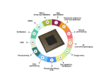
A typical upstream end transceiver is shown in first figure with high speed components omitted for clarity. By upstream, we mean the end nearer to the host. The upstream end has two 15K pull-down resistors.
Each line can be driven low individually, or a differential data signal can be applied. The maximum ‘high’ level is 3.3V.
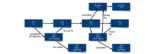
The equivalent downstream end transceiver, as found in a device, is shown in second figure.
When receiving, individual receivers on each line are able to detect single ended signals, so that the so-called Single Ended Zero (SE0) condition, where both lines are low, can be detected. There is also a differential receiver for reliable reception of data.
Some signaling that the transceiver need to be aware is described below:
At the device end of the link a 1.5 kohm resistor pulls one of the lines up to a 3.3V supply derived from VBUS.
This is on D- for a low speed device, and on D+ for a full speed device.
(A high speed device will initially present itself as a full speed device with the pull-up resistor on D+.)
Given that there are just 2 data lines to use, it is surprising just how many different conditions are signaled using them:
When no device is plugged in, the host will see both data lines low, as its 15 kohm resistors are pulling each data line low.
When the device is plugged in to the host, the host will see either D+ or D- go to a ‘1’ level, and will know that a device has been plugged in.
The ‘1’ level will be on D- for a low speed device, and D+ for a full (or high) speed device.
The state of the data lines when the pulled up line is high, and the other line is low, is called the idle state. This is the state of the lines before and after a packet is sent.
To make it easier to talk about the states of the data lines, some special terminology is used. The ‘J State’ is the same polarity as the idle state (the line with the pull-up resistor is high, and the other line is low), but is being driven to that state by either host or device.
The K state is just the opposite polarity to the J state.
The Single Ended Zero (SE0) is when both lines are being pulled low.
The J and K terms are used because for Full Speed and Low Speed links they are actually of opposite polarity.
All details is shown in the figure below:
This is the illegal condition where both lines are high. It should never occur on a properly functioning link.
When the host wants to start communicating with a device it will start by applying a ‘Reset’ condition which sets the device to its default unconfigured state.
The Reset condition involves the host pulling down both data lines to low levels (SE0) for at least 10 ms. The device may recognise the reset condition after 2.5 us.
The End of Packet (EOP) is an SE0 state for 2 bit times, followed by a J state for 1 bit time.
One of the features of USB which is an essential part of today’s emphasis of ‘green’ products is its ability to power down an unused device. It does this by suspending the device, which is achieved by not sending anything to the device for 3 ms.
Normally a SOF packet (at full speed) or a Keep Alive signal (at low speed) is sent by the host every 1 ms, and this is what keeps the device awake.
A suspended device may draw no more than 0.5 mA from Vbus.
A suspended device must recognise the resume signal, and also the reset signal.
When the host wants to wake the device up after a suspend, it does so by reversing the polarity of the signal on the data lines for at least 20ms. The signal is completed with a low speed end of packet signal.
This is represented by a Low speed EOP. It is sent at least once every millisecond on a low speed link, in order to keep the device from suspending.
SIE
What is the SIE? A typical function USB hardware interface is shown below
The SIE is the frontend of this hardware and handles most of the protocol signaling. The SIE typically comprehends signaling up to the transaction level. The functions that it handles could include:
- Packet recognition, transaction sequencing
- SOP, EOP, RESET, RESUME signal detection/generation
- Clock/Data separation
- NRZI Data encoding/decoding and bit-stuffing
- CRC generation and checking (Token and Data)
- Packet ID (PID) generation and checking/decoding
- Serial-Parallel/ Parallel-Serial Conversion
A typical implementation of an SIE with these functions takes about 2500 gates. So the module itself is fairly small; and the functionality is straightforward. In spite of this apparent simplicity, it is possible to end up with a design that doesn’t work reliably i.e. a design which is not robust. I will point out some reasons for problems from a design.
- Sources of robustness problems
The primary source of robustness problems is the existence of multiple clock domains in the SIE, some of which are asynchronous to each other. If signaling between these domains doesn’t adhere to synchronization rules, intermittent problems can result. These problems are invariably difficult to track down and fix.
Other areas which have the potential for robustness problems include:
- out-of-band signal handling on per-packet basis
- bit stuffing/unstuffing
- special casing for setup, iso etc
- special casing for low speed
- suspend /resume support
The following text will review some of these areas in turn and discuss techniques to address the problems.
The typical SIE has to deal with four clock zones in three domains:
- · USB host 12Mhz clock or receive clock
- · internal 4x clock (48Mhz) and transmit clock (divided by 4 version)
- · SIE backside clock or interface clock
- Race Conditions in the transmit domain
The clock zones in the second domain are synchronous; however race conditions could occur in signaling between the 1x and 4x sub domains because the 1x clock is derived from the 4x clock. This may be a bigger problem in some target technologies than in others. The problem is exacerbated by the need to switch the hardware between transmitter and receiver clocks.
Since the USB is half duplex several of the modules in the SIE can be shared between transmit and receive e.g. the crc logic . Since every USB transaction includes receive and transmit phases, the state machines carry state between the phases. So there is a need for a means to reliably multiplex between receive clock and transmit clock.
- Packet delimiters and out of band signaling
Precise detection of packet delimiters is crucial for robust SIE operation. Each packet has a start delimiter (or sync) and end delimiter (or EOP). The nominal sync field consists of an NRZI KJKJKJKK pattern. Even though this is an in band (made up of differential signals) pattern, the initial bit may be distorted due to hub turn on behavior .
- Bit stuffing and unstuffing
Bit stuffing and unstuffing can be implemented by putting the state machines and datapath on hold while stuffing or stripping the extra bit. Bit unstuffing near the EOP needs to be handled carefully as explained above.
Although most transactions are three phase, ISO transactions are only two phase and the state machines need to comprehend this. Similarly SETUP transactions are identical to OUT transactions except that they cannot be NAKed or STALLed. The data buffering and the state machines need to take this into account. Data toggle sequencing logic at a bidirectional endpoint should take into account the specific requirements for the starting toggle sequence of each stage of a control transfer.
Low speed signaling is identical to full speed signaling except for the inversion of polarity. But low speed devices need to comprehend that while most data entities are defined in terms of number of bits, the se0 width for reset is not. Low speed devices should also be able to handle keep-alive signals (bare EOPs) correctly.
USB Protocol in Depth – Protocol Layer
In this article I’ll try my best to explain the most part of the protocol layer of USB specification.
I’ll talk a little about the transfers, but will not cover a lot, maybe I’ll make an article just about the transfers, but what you need to know is that for each use you have a different type of packages.
In the last section we could check the physical layer that will interface the connector and will work together with the SIE, but as the SIE isn’t very well define in the specifications this could lead to great confusion, as many manufacturers could implement the SIE together with the Protocol layer, or some of the functions of the protocol.
As what I define about SIE in the last post, SIE will handle the signaling and the interface with protocol layer, to let things easier let’s consider that the SIE will interface with protocol layer by UTMI (USB 2.0 Transceiver Macrocell Interface) or ULPI (UTMI+ low pin interface), that’s the usually you can find in most standard USB 2.0/3.0 transceiver integrated circuits.
Other consideration is that I’ll need to define the 4 types of transactions that exists on USB protocol:
- Control Transfers Used for sending commands to the device, make inquiries, and configure the device.
- Interrupt Transfers Used for sending small amounts of bursty data that requires a guaranteed minimum latency.
- Bulk Transfers Used for large data transfers that use all available USB bandwidth with no guarantee on transfer speed or latency.
- Isochronous Transfers Used for data that requires a guaranteed data delivery rate. Isochronous transfers are capable of this guaranteed delivery time due to their guaranteed latency, guaranteed bus bandwidth, and lack of error correction. Without the error correction, there is no halt in transmission while packets containing errors are resent.
The protocol layer manages the end-to-end flow of data between a device and its host. This layer is built on the assumption that the link layer guarantees delivery of certain types of packets and this layer adds on end to end reliability for the rest of the packets depending on the transfer type.
Here we will discuss the following concepts in detail:
- Types of packets
- Format of the packets
- Expected responses to packets sent by the host and a device
- Support for Streams for the bulk transfer type
- Timing parameters for the various responses and packets the host or a device may receive or transmit
One first thing if you look at the USB communication from a time perspective, it contains a series of frames, in your time slot. Each frame consists of a Start of Frame (SOF) followed by one or more transactions. Each transaction is made up of a series of packets. A packet is preceded with a sync pattern and ends with an End of Packet (EOP) pattern. At a minimum, a transaction has a token packet. Depending on the transaction, there may be one or more data packets and some transactions may or may not have a handshake packet.
Packet Types can potentially represent four packet types:
1. Token packets
- Initiate transaction
- Identify device involved in transaction
- Always sourced by the host
2. Data packets
- Delivers payload data
- Sourced by host or device
3. Handshake packets
- Acknowledge error-free data receipt
- Sourced by receiver of data
4. Special packets
- Facilitates speed differentials
- Sourced by host-to-hub devices
I’ll cover Token, Data and Handshake packets, special packets will be cover maybe in a future article about Hubs, leave a comment if you want an article about USB HUB.
Token packets always come from the host and are used to direct traffic on the bus. The function of the token packet depends on the activity performed, the format for a token packet is shown in the image below.
Another token packet is a SOF (start of frame) packet, show in the figure below
Data packets follow IN, OUT, and SETUP token packets. The size of the payload data ranges from 0 to 1024 bytes depending on the transfer type. The packet ID toggles between DATA0 and DATA1 for each successful data packet transfer, and the packet closes with a 16-bit CRC. The format is shown in the figure below
Handshake packets conclude each transaction. Each handshake includes an 8-bit packet ID and is sent by the receiver of the transaction, the format is shown in figure below
I know that I’m missing more information about each bit in PID, ADDR, ENDP, DATA, Frame Number and CRC5/16, but this article is already to extensive, if you want know more details, leave a comment.
How the USB is a protocol with handshake, usually with some packets will be expect some responses, to simplify let’s consider that always an token will be sent, followed by a data packet or receiving a data packet always will be a handshake packet involved, how the article is going a little extend, leave a comment if you want an article about the transfers.
All this is valid for each type of transfers, which can be a control, interrupt, bulk or isochronous transfers.
Other concept is that each 1ms is a frame that contain a SOF and can contain many packets. In high speed an SOF is sent out every 125 us and frame count is only incremented every 1ms.
USB in Depth – xHCI


