
We take for granted today the staggering precision of modern technology. Cars, electronics, robots and medical equipment, all come off the factory floor composed of effortlessly interchangeable parts; but this was not always the case. In the late 18th century most things that required any kind of precision were made by hand, one notable example being the flintlock musket. You see back then if you wanted a rifle you ordered one from a gunsmith, and he built for you, by hand, an essentially custom (bespoke) product. If something broke you took it back to a gunsmith who would craft a repair for that particular rifle – you couldn’t swap out a part with a replacement because at that time parts weren’t interchangeable. At least not until Honoré Blanc showed us all it could be done. So while my last blog was focused on the verification challenges of the Pilgrims, and my next blog returns to the sea to show how the unrelenting determination of one self-taught genius saved untold lives. Today we focus on one lone gunsmith… in a dungeon.
He made guns, in prison?!?
Blanc wasn’t the first to think of, or even implement interchangeable parts, but he was the first to do it for something as complicated as a flintlock musket. He did it to drive efficiency, enable in-field repairs, and…well, actually, no. At the time the cost and reliability issues were causing friction between the French Army and the gunsmiths, who were choosing to sell their guns to the Americans and thus causing gun shortages in France. A solution was needed to allow for less-skilled craftsmen to assemble their guns, and that was the nexus of the interchangeable flintlock musket! And that was also the reason that Honoré Blanc had to carry out his work in the dungeons of a castle, as a means of protection from his fellow gunsmiths (and I’m guessing if there was a profession you did not want to aggravate, it would be gunsmiths!).
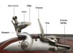
Flintlock mechanism – source Wikipedia.org
Now THAT’S how you do a demo!
After developing the means and technology to enable interchangeable parts for his flintlock rifles, Honoré risked the wrath of the Demo Gods by demonstrating his approach in a spectacular manner. Surrounded by dignitaries and officials, including a young American Minister to France named Thomas Jefferson, Honoré produced 50 locks (the firing mechanism at the heart of a flintlock musket), calmly disassembled half of them, threw their parts into boxes, casually mixed them, and just as calmly pulled random parts and reassembled the locks. It was an absolutely unbelievable display at the time and earned him a contract to put his idea into practice (and a revered place in history).
But implementation is hard, always has been…
Sadly for Honoré political pressure and the destruction of his workshop in the French Revolution meant he was never able to mass produce his locks at a low-enough cost, and ultimately the gunsmiths won the battle over interchangeable parts and the technology was lost to France for decades. If he had only known about Shropshire’s own (hey, this is a British blog, we were bound to get back here at some point!) John “Iron-Mad” Wilkinson who, a decade before, had invented a method of boring a true and straight hole in cannon-shaped lump of metal and later applied that to the problem of less-than true and round cylinder panels in steam engines. Wilkinson had essentially built a tool to automate a manufacturing process, something Blanc desperately needed.
But remember that young American dignitary? He saw the potential of the technology, and after failing to convince Blanc to move to the US brought back the idea and samples and set up armouries intended to prove out the interchangeable parts approach. Later at one of the armouries, John Hancock Hall realised that this was in fact a precision game (on the order of tenths of a millimetre) and developed measurement techniques and machines to enable completely interchangeable locks. Eventually a contract for 10,000 muskets was given to Eli Whitney (yes, that Eli Whitney) on the strength of his demonstration of interchangeable parts. But Whitney would be many years late on his promised delivery; he had in fact needed the money because of the debt incurred while litigating the patents on his cotton gin, and eventually would be discredited as his “demo” was found to be rigged!
But that was then, and we’ve solved the precision problem, right?
Even though in modern ASIC’s we are dealing now with billionths of a meter (Moortec has announced support for TSMC’s 5nm process), that in no way means we have solved the precision problem. Just as metals can warp, get knocked out of true, or suffer from manufacturing discrepancies, the silicon our electronics are built from can also warp during slicing of the wafers into die, get knocked around during packaging, or suffer from process variation. But unlike gunsmiths of the 18th century, modern engineers now have amazing tools at their disposal, tools that allow them to monitor what’s happening inside their devices in real time and to see exactly what the variances from spec and impacts are. The choice is simple…either know for a fact that there are potential problems lurking and willingly decide to ignore them, or know exactly what is happening on your device using the best tools and IP available.
I know which one I would choose if tens of millions of development dollars were on the line…
In case you missed any of Moortec’s previous “Talking Sense” blogs, you can catch up HERE.


