Anna has more than 25 years of expertise in managing complex R&D organizations and programs, giving birth to a number of innovative EDA technologies. She has pioneered the study and development of several generations of IC and package co-design environments and has held senior positions at leading semiconductor and EDA company including STMicroelectronics and Mentor Graphics.
Candidly, I’ve never heard of Monozukuri. Why are you guys suddenly emerging from stealth mode?
Great question. Since establishing Monozukuri in 2014, we’ve spent all of our time defining and refining our IC/package co-design system technology with a team whose broad experience stretches across system architecture, IC design and IC package design. The team, including myself, comes from ST Micro and Mentor. We used this time to really study the challenges. Rather than bolt something on to an existing tools, we took the time to build a revolutionary new design platform from the ground-up.
Clearly, making promises or prematurely hyping our direction would have been counter-productive until products were fully ready. So we quietly did the hard work and the result are a product line and a technology platform dedicated to support 3D system co-design
And, most importantly, the products are available for licensing now.
Why is advanced packaging so important to the future of IC design?
I think the semiconductor industry is transitioning from ‘Moore’s law’ to ‘More than Moor’s law.’ So if designers are going to incorporate more functionality into smaller spaces, they’ll be beyond a single piece of silicon. The next logical extension is to integrate multiple devices in a commercially-compelling, space-saving wrapper that optimizes system performance.
That what 2.5/3D heterogeneous integration is all about. Each silicon component can target the ideal PPA manufacturing node. Expensive latest technology can be reserved for only the most aggressive digital demands, while the remaining ICs (including a silicon interposer) can target more cost and performance-efficient options.
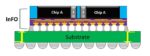
Advanced AI system, networking products, cell phones, and wearable devices all require highly complex, small form factor systems. Emerging 2.5/3D packages integrate highly complex multi-chip solution with tens of thousands of connections that support massive, high-speed data in a space-optimized system.
GENIO is your first co-design system. What are some its features?
GENIO provides a holistic design environment for 2D, 2.5D and 3D multi-component systems. GENIO is actually a suite of tools that generates new levels of performance in terms of speed, optimization efficiency, and system performance.
GENIO generates system design across multiple levels and components including die, chiplet, silicon interposer, package, and PCB. It’s proven to eliminate dead end architectures and ensures first-time-silicon success.
The GENIO suite uses standard formats to seamlessly integrate with all existing commercial implementation platforms or dedicated plug-ins to integrate into custom EDA flows. Its graphic interface provides an immersive 3D interactive visualization of the complete system. GENIO’s architecture also enables new standard and customized features that support both evolving tool environments and proprietary customer-specific requirements.
Which one feature do you believe is absolutely key to the future of Co-design ?
I believe that true system co-design must be created from concept to completion by including all components from board level to chip level within the same seamless, comprehensive environment.
GENIO allows designers to consider all system components from initial high level system design exploration to detailed system integration and optimization. This is what enables design across multiple levels and components.
A larger competitor announced that they are working on a co-development tool, yet you’re announcing GENIO is available now. How did you get to market so quickly?
We’re seeing larger EDA companies racing to address co-design by evolving and adapting existing IC and package design tools. That approach severely compromises overall systems functionality.
At Monozukuri, we’ve been ahead of the game since 2014. That’s why today, we’re delivering … and I emphasize delivering … a ground-up, integrated technology that embraces all of the demands of complete 3D system co-design.
We’re able to do this because GENIO is completely unconstrained. What I mean is that GENIO works with all system components from board to chip because we built it from the ground up. It’s completely agnostic to surrounding EDA tools and it interfaces with almost all IC and package physical design tools.
You keep emphasizing immediate availability. Where’s the data to back that up?
Over the past 12 month we’ve demonstrated GENIO to multiple customers and have run a number of custom optimizations.
For instances, we successfully completed a 2.5D system feasibility analysis in 6 hours that previously took three entire teams … one for architecture, one for backend and one for package … 15 days. That’s literal a 99.95% reduction in design time, with an associated 99.95% cost savings.
Another customer used GENIO to determine in four hours what a manual solution couldn’t accomplish in two weeks: Discovering that a proposed IC/packaging system architecture wouldn’t work.
Finally, GENIO optimized a 2.5D HBM-based design that included a complex hierarchical ASIC … multiple hard-IP, plus multiple soft IP, plus probe pads and a complex P&G pins scheme .. using recursive methodology within 8 hours. While the customer didn’t disclose the cycle time, we believe their traditional methodology would have taken around 45 days.
What’s the roadmap for GENIO? When can we expect to see a full 3D tool?
Today we have a 2D and 2.5D solutions available. The 3D platform is in final stage beta testing and is scheduled for release in the 4th quarter.
GENIO 3D includes three features essential for complete system I/O optimization: First, the ability to manage component placement priority within the 3D stack at the architectural exploration stage. Second, TSV location management to meet manufacturing and/or customer-specific constraints. And last, complete through-stack optimization to minimize TSV population whilst managing system optimization to lessen TSV yield impact .
This is a huge undertaking and you certainly haven’t been on the VC map. Where did you get your funding?
We financed the company using European and Institutional private equity. Through this funding we were able to complete proof-of-concept and early product development.
However, the majority of funds has come from project grants associated with European research program. Through our participation in the Horizon 2020 program we not only made significant contributions to European research, but also used the findings to complete tool development and get ourselves ready to market.
Where to from here? When can we expect to hear more from Monozukuri?
Actually, now that we’re negotiating initial licenses, you’ll probably see a great deal of us. While we were in stealth, we felt it necessary to decline a number of invitations to discuss our technology platform and some of the co-design challenges we all face. Now, we’re wide open to discussing what we see as the barriers and opportunities along the co-design frontier. We already shared our short-term roadmap, and we look forward to upholding our role as co-design innovator.
Also Read:
CEO Interview: Isabelle Geday of Magillem
CEO Interview: Ted Tewksbury of Eta Compute
CEO Interview: Ljubisa Bajic of Tenstorrent


